4–20 mA Gateway Inputs: Budget the Loop Voltage Before Choosing the Shunt
A current-input gateway can pass a short-cable bench demonstration and still flatten the top of a transmitter’s range after installation. The temptation is to investigate ADC scaling first. A more useful first question is whether the transmitter still has enough terminal voltage to regulate the requested current. Adding a gateway to an existing loop is an electrical load change, not merely a software integration.
This article develops a proposed acceptance method for a custom industrial input board. The numerical example is a design calculation, not a field measurement or a specification for a particular transmitter. Texas Instruments’ TIDUAM6 reference-design guide, dated October 2015, provides the underlying distinction: receiver resistance consumes loop voltage, while the transmitter needs a minimum terminal voltage to remain within specification.
Start with the complete series path
Draw the actual current path before choosing an ADC gain. Include the power supply, transmitter, outgoing and return conductors, existing receiver, proposed gateway shunt, and every series protection element. Label which devices supply energy and which only receive current. This article assumes a two-wire, loop-powered transmitter and a passive gateway input. An actively powered input requires a different wiring review; two sources must not be casually connected together.
The useful design inequality is:
V_supply_min − I_max × R_series_total − V_other_drops ≥ V_transmitter_min.
All terms refer to the same worst-case operating condition. R_series_total includes both cable conductors and all resistive burdens. V_other_drops covers separately characterized nonresistive drops. The transmitter’s minimum voltage comes from its own documentation, not from the gateway designer’s preferred nominal supply. Use the highest current the product must receive, including any supported overrange or diagnostic level, rather than assuming that 20 mA is always the limit.
An illustrative budget exposes the tradeoff
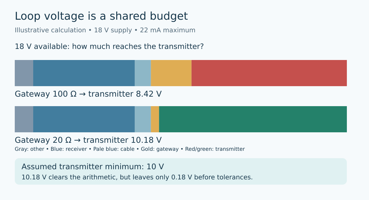
Suppose the installation is designed around an 18 V minimum supply, an assumed transmitter requirement of 10 V, and a required maximum current of 22 mA. Assume another 1 V is reserved for characterized series drops. These are example inputs chosen to show the method.
The remaining resistive allowance is 7 V divided by 0.022 A, approximately 318 Ω. If the existing receiver uses 250 Ω and the cable pair contributes 40 Ω, only about 28 Ω remains before consuming that allowance. Adding a 100 Ω gateway shunt produces 390 Ω total. At 22 mA its resistive drop is 8.58 V, leaving 8.42 V for the transmitter after the assumed 1 V drop. That fails the example’s 10 V requirement.
A 20 Ω gateway shunt instead gives 310 Ω total and leaves 10.18 V. The arithmetic passes, but the 0.18 V margin is too small to declare a robust design without tolerances, temperature effects, supply behavior, and further installation requirements. This distinction matters: passing a nominal inequality is not the same as accepting a product.
Lower burden moves work into the analog front end
Reducing the shunt from 100 Ω to 20 Ω reduces the nominal 20 mA signal from 2 V to 0.4 V. That preserves voltage for the transmitter but changes the signal-conditioning problem. The ADC range, amplifier offset, input noise, reference error, and board leakage must now be evaluated against the smaller signal. Resolution alone cannot establish accuracy.
The board review should therefore carry two linked budgets: available loop voltage and input measurement error. A large shunt can simplify one while breaking the other. Shunt tolerance and temperature coefficient belong in the measurement budget; shunt maximum resistance also belongs in the voltage budget. Protection should be evaluated as part of the channel, not attached after both budgets have been declared complete.
If there is an existing receiver, investigate whether a suitable isolated acquisition approach can observe its signal without adding an unacceptable series burden. Do not assume that sharing a ground or connecting an ADC across another instrument’s resistor is permissible. Common-mode range, isolation requirements, fault paths, and ownership of the original instrumentation remain explicit design inputs.
Build an acceptance fixture that changes the constraint
A useful test fixture makes supply voltage and series resistance adjustable independently. First characterize the gateway using a suitable current source within its operating limits. Then test the intended transmitter and receiver combination with a controlled series resistance representing the installation. Record supply voltage, actual loop current, transmitter terminal voltage, and gateway conversion together.
Sweep the required input range at the minimum specified supply. Repeat at the maximum permitted cable resistance and with the specified existing burden. Include the application’s supported overrange current. The pass condition is not simply a plausible digital number: the physical loop current must track the demanded condition, and the gateway must measure that current within its allocated error.
When the top of the range flattens, compare the transmitter terminal voltage with its requirement before recalibrating software. Otherwise a calibration correction may conceal a wiring-dependent limitation at one test point while making other conditions worse. Keep raw readings and fixture settings with the report so another engineer can distinguish acquisition error from a transmitter that has already run out of voltage.
Make the integration contract installable
The product handoff should specify the permitted loop topology, maximum gateway burden, accepted current range, common-mode and isolation boundaries, and required supply calculation. Give installers a worksheet with explicit spaces for the existing receiver and the cable pair. A statement such as “supports 4–20 mA” does not tell them whether the channel can be inserted into their loop.
For an Obeita custom gateway project, this is a concrete hardware acceptance deliverable: a schematic-level burden budget connected to an executable bench plan. It prevents a cloud dashboard from receiving beautifully formatted measurements from a physically constrained loop. No testing or certification is claimed here; the example identifies what must be measured and documented before release.
Source and topic provenance
Technical foundation: Texas Instruments, TIDUAM6, October 2015, section 4 and the loop discussion on printed page 9: Texas Instruments TIDUAM6, October 2015, printed page 9
Topic selection uses the preserved Google Trends RISING row “industrial iot solutions,+110%,” Worldwide, all categories, web search, July 19–October 19, 2026. This supports the parent industrial-IoT topic only; it does not establish search growth for this title or its engineering terms.