Gateway Switchers: Bootstrap Refresh Limits Near Dropout
A buck converter can appear to have enough input voltage for a gateway rail yet stop regulating during a lightly loaded interval. One possible cause is not output-current demand but high-side gate-drive energy. A bootstrap supply must maintain voltage above the switching node, and its recharge opportunity can become restricted when the converter spends nearly all its time on.
The concrete reference is Texas Instruments’ TPS57060-Q1 datasheet, SLVSAP2C, revised February 2016, section 7.3.3 on page 13. The device example and the independent simplified calculations below have different scopes: the calculations explain boundaries and are not a simulation or guaranteed model of that regulator.
Reference the gate drive to the switching node
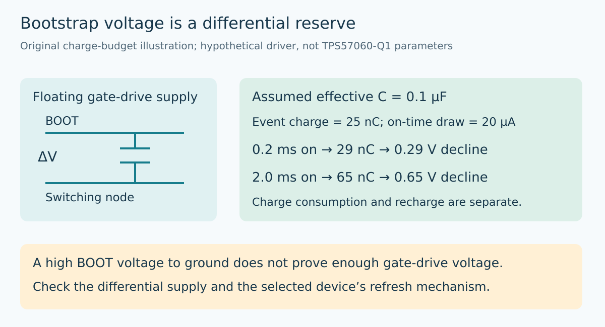
An N-channel high-side MOSFET needs gate voltage above its source, which is the switching node in a buck stage. A bootstrap capacitor provides a floating energy reservoir for that driver. Its useful voltage is the difference between the bootstrap and switching-node pins, not the bootstrap pin’s voltage relative to ground.
A scope trace that shows the bootstrap node moving high can therefore be misleading. The two nodes may rise together while the differential voltage that powers the driver is becoming inadequate. Probe that differential with an appropriate measurement method and respect both differential and common-mode ratings.
On a conventional bootstrap arrangement, the recharge path becomes available while the switching node is sufficiently low. The actual path depends on the regulator’s topology, internal charging circuit, and low-side behavior. A synchronous converter, a diode-based converter, and a device with an auxiliary charge pump must not be assigned the same recharge rule.
Separate charge consumption from recharge opportunity
A simplified charge budget can include the gate-driving event, floating-driver consumption during the on interval, and leakage. The approximate bootstrap-voltage loss is total consumed charge divided by effective bootstrap capacitance. This is a useful bookkeeping relationship, not a replacement for the vendor’s capacitor recommendation.
For a hypothetical driver unrelated to the specified TPS57060-Q1 parameters, assume 25 nC of event-related charge, 20 µA of sustained consumption, and 0.1 µF effective capacitance. A 2 ms on interval adds 40 nC of consumption, producing 65 nC total and a calculated 0.65 V decline. A 0.2 ms interval produces 29 nC total and a 0.29 V decline.
The example makes the distinction visible: switching-event charge and elapsed-time consumption are different terms. The real circuit must also recharge the reservoir through a finite path. Increasing capacitance can reduce a single-event voltage change while changing recharge behavior; it is not automatically an approved cure.
Understand what “100% duty” means for the selected device
The TPS57060-Q1 specifies a 0.1 µF bootstrap capacitor and describes extended high-side on operation while BOOT-to-PH voltage remains above its stated 2.1 V threshold. Its control interrupts that interval when refresh is needed. This is not an unlimited promise that the high-side device can remain on forever.
At light or zero load, the datasheet warns that insufficient inductor current may prevent the switching node from falling enough to replenish the bootstrap capacitor. Output voltage can then decay before switching resumes. That documented operating condition is why a full-load dropout check alone is insufficient.
Keep the manufacturer’s typical curves in their proper role. They illustrate behavior for the stated conditions, not guaranteed start and stop thresholds for every layout, component tolerance, and temperature. Where a design requires a hard boundary, use documented limits and validation appropriate to that requirement.
Do not confuse this with minimum on-time
At a high input-to-output ratio, a buck converter may need pulses shorter than its minimum permitted on interval. Near dropout, the problem is at the opposite end of the duty range: preserving off or refresh opportunities while maintaining output voltage. The remedies and test corners are different.
For a separate hypothetical fixed-frequency converter that requires 100 ns off time each cycle at 500 kHz, the maximum nominal duty would be 95%. Ignoring losses, a 5 V output would then need at least 5 / 0.95, approximately 5.263 V input. That elementary limit is not the TPS57060-Q1 control law, which can extend on intervals and refresh differently.
The comparison is useful during part selection. Determine whether the candidate has a fixed minimum off time, periodic refresh, a charge pump, or another specified dropout mechanism. Do not apply a convenient duty-limit equation until its assumptions match the actual architecture.
Test the gateway’s quiet intervals
An industrial gateway may reduce activity after a radio transmission or disable sensor channels between scans. That lighter load can expose bootstrap behavior that is absent during a sustained workload. Include transitions into and out of the minimum supported load, not only maximum current.
Use a slow input sweep where permitted, then add controlled input disturbances representative of the supported source. Capture input voltage, output voltage, switching-node activity, and bootstrap differential voltage together. A long enough record is needed to reveal refresh bursts and intervening output decay.
Choose observation thresholds before collecting traces: minimum acceptable output, allowed interruption duration, and the downstream reset boundary. Distinguish loss of regulation from a harmless change in switching pattern. An unusual waveform is not a failure unless it violates a documented electrical or functional requirement.
Resolve the boundary without disguising it
Possible design decisions include maintaining more input headroom, setting a justified undervoltage stop point, or selecting a regulator with a dropout architecture suited to the load envelope. A permanent preload may alter behavior but consumes power and needs its own thermal and operating justification.
Do not change the bootstrap capacitor outside supported guidance merely because one trace improves. Recheck startup, recharge, supported switching modes, and relevant absolute maximum limits. The release evidence should identify the exact device revision and the load/input combinations actually covered.
A reliable gateway power stage needs both energy at the output and energy for the switch that delivers it. Treat bootstrap refresh as a separate operating constraint, and the apparently contradictory result of a regulator failing at light load becomes a testable circuit question.
Topic provenance
The preserved Google Trends RISING row “industrial iot solutions,+110%,” worldwide, all categories, web search, July 19–October 19, 2026 supports the parent integration topic only. It does not establish search growth for this electrical mechanism or article title.