Flash Read-While-Write Constraints: Keep Interrupts and Code Fetch Safe During Programming
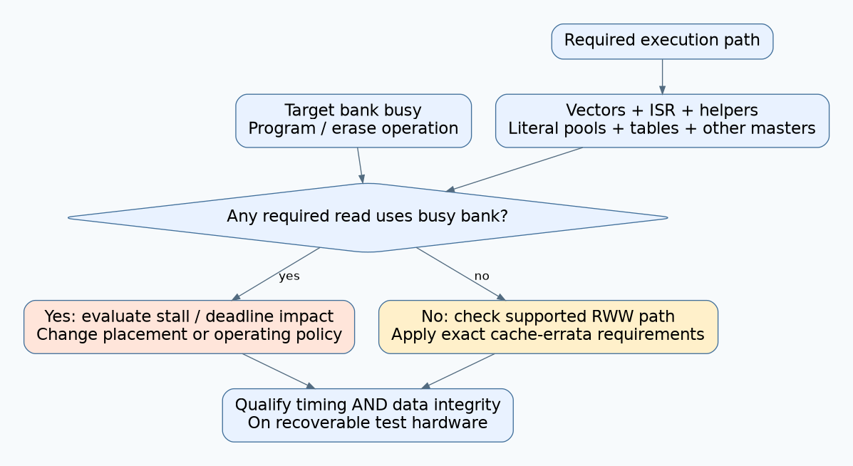
Programming internal flash can block execution that still needs the affected flash bank. Moving one programming function to RAM is not enough if an interrupt vector, handler, helper function or constant remains in that bank. Qualify the complete access dependency path and the exact device’s concurrent-operation rules.
The concrete example is a 2-Mbyte STM32F429 dual-bank configuration, using RM0090 revision 22, DS9405 revision 14 and ES0206 revision 24. This is not a rule for all STM32 devices or all memory densities. Confirm the actual part, silicon revision, bank arrangement and deployed driver before applying it.
1. Start from the documented bank restriction
RM0090 section 3.6 describes stalling reads during flash programming or erasure, with the dual-bank exception allowing reads from one bank while the other is being programmed or erased. Section 3.6.5 also excludes concurrent write/erase activity in both banks. Read-while-write is not write-while-write.
The STM32F427xx/429xx datasheet identifies the device family and memory options. Its flash programming tables distinguish operation types, sector sizes and program/erase parallelism. Use the applicable maximum and conditions when budgeting a blocked interval; a short typical programming time does not bound every erase operation.
A stall and a CPU fault are different outcomes. Do not infer that a missed deadline means the processor executed corrupted instructions, or that the absence of an exception proves the deadline was met. Record both timing behavior and integrity results.
2. Build a map of every access needed during the operation
| Dependency | Evidence to inspect | Common hidden access |
|---|---|---|
| Flash-operation routine. | Final linked address and disassembly. | A called helper remains in the busy bank. |
| Interrupt entry. | Active vector-table location and handler address. | The handler moved, but its vector did not. |
| Handler dependencies. | Call graph, literal pools and read-only data. | A lookup table or format string is still in flash. |
| Scheduler and fault paths. | Actual paths allowed during the operation. | A context switch or error report enters the busy bank. |
| Other bus masters. | DMA/peripheral access map and device rules. | A transfer sources data from the affected flash region. |
| Watchdog/progress checks. | Execution path and permitted timing window. | The monitoring code cannot run while the bank is busy. |
Use the final ELF, linker map and generated configuration. Source annotations show intent, while linking, optimization and library selection determine actual placement. Inspect veneers, inlined code and out-of-line library calls instead of assuming a function’s section annotation covers everything it reaches.
If RAM execution is selected, confirm that the chosen memory is executable and initialized before use under this device’s memory map. “RAM” is not a sufficient placement specification. Startup copying and cache behavior belong in the qualification record.
3. Choose an execution policy that meets the deadline
- Allow a bounded stall: only when every affected product deadline and watchdog constraint can tolerate the documented operation envelope.
- Execute from the other bank: only when all required code and data accesses remain supported while the target bank is busy.
- Use a complete RAM-resident path: include its vectors, handlers, helpers and data dependencies where needed, not just the low-level writer.
- Schedule a maintenance interval: explicitly pause or reject time-sensitive product work under an approved operating policy.
Do not disable interrupts or supervision merely to make a programming demonstration pass. Interrupt masking changes the product’s responsiveness and can hide the exact workload the test needs to evaluate. Any intentional restricted interval needs an accepted duration and recovery behavior.
4. Review cache limitations before claiming dual-bank safety
ES0206 revision 24, section 2.2.15, documents possible data-cache corruption during dual-bank read-while-write with the data cache enabled. It supplies a workaround involving disabling the data cache before the affected write and resetting it before reenabling. Match the complete documented conditions and sequence to the actual driver; this article is not a register-programming recipe.
A successful run with warm caches can also conceal dependencies on the busy bank. Qualification should exercise representative cache states and branch paths through the supported platform controls. Do not rely on a tiny loop staying cached as proof that every interrupt and error path remains available.
Keep timing restrictions and data-integrity restrictions separate in the report. Other-bank execution can address a bank-access stall while an applicable erratum still requires its own handling. Review the complete device errata for the selected silicon revision rather than stopping at the RWW headline.
5. Design a programming-under-load test
Use recoverable development hardware with a documented recovery path and an explicitly sacrificial flash region. Preserve valuable data and verify that test sectors do not contain the bootloader, active image, calibration or credentials. This article includes no erase/program commands and reports no hardware execution.
- Record the exact image hash, linker map, bank map, part marking and silicon revision.
- Run a baseline periodic workload without flash operations, using an independent timing observation.
- Exercise the permitted program and erase operations in the sacrificial region while the workload and relevant interrupts run.
- Measure operation start/end, interrupt-entry delay, completion delay, missed events and data correctness.
- Repeat across the supported execution-placement cases, sector sizes, cache conditions and operating envelope.
- Exercise the timeout/error path and confirm it does not depend on the resource whose availability is being tested.
Use hardware timing capture or another observation that remains meaningful when CPU execution stalls. A software timestamp written only after the stall can hide when an event actually arrived. Avoid logging test results to the same flash path during the critical interval.
6. Interpret the result with the dependency map
If both foreground code and an ISR pause until flash completion, inspect their shared bank dependencies. If only one handler stalls, compare its vectors, helpers and constant data with a handler that continues. If timing is acceptable but a value changes unexpectedly, investigate applicable cache behavior and integrity checks rather than declaring the test successful.
Define release criteria before measuring: permitted worst-case service delay, no lost required events, correct programmed/read-back contents, preserved unrelated regions and a working error path. Average latency is insufficient for a deadline that must hold throughout the operation.
Hypothetical hidden constant
A test build places an interrupt handler in SRAM, but the handler reads a lookup table linked into the bank being erased. The handler’s address looks correct while its dependency still blocks. Moving or otherwise avoiding that dependency under the supported memory policy is the issue to qualify, not merely increasing the task priority.
Release the bank/access map with the exact device documents, errata disposition and load-test evidence. Storage concurrency is a hardware access contract that must be reflected in the final linked firmware.