STM32WB HSE Trimming: Turn a Prototype Setting into a Production Accuracy Budget
A useful HSETUNE value on one STM32WB55 prototype is not automatically the best fixed value for a production design. ST documents board-to-board frequency variation at the same trim setting and proposes a sample-based method for choosing a shared setting. The residual variation must remain in the RF carrier-accuracy budget.
This article follows AN5042 Rev 16, AN5378 Rev 3 and the WB55 datasheet. It describes a qualification method; it contains no measured production distribution and does not program calibration storage.
Separate centering from the complete accuracy requirement
AN5378 section 6 explains that WB devices use an external 32 MHz crystal and internal programmable capacitance to tune its frequency. Board parasitics affect the result, so the crystal's nominal frequency alone does not establish the assembled oscillator's center frequency.
AN5042 section 1.8 treats frequency tolerance, temperature behavior, aging and pullability as contributors to carrier accuracy. Trimming the room-temperature center removes neither temperature variation nor aging over the product's intended life.
Use the WB55 datasheet for the actual oscillator conditions and device limits. A typical trim granularity or an application-note example is not a guaranteed residual error for every board and environment.
The distinction changes the acceptance question. “Can I tune this specimen close to 32 MHz?” concerns centering. “Does the design remain within its applicable requirement across production and operating conditions?” requires the wider budget.
Apply ST's production method to the design, not an isolated board
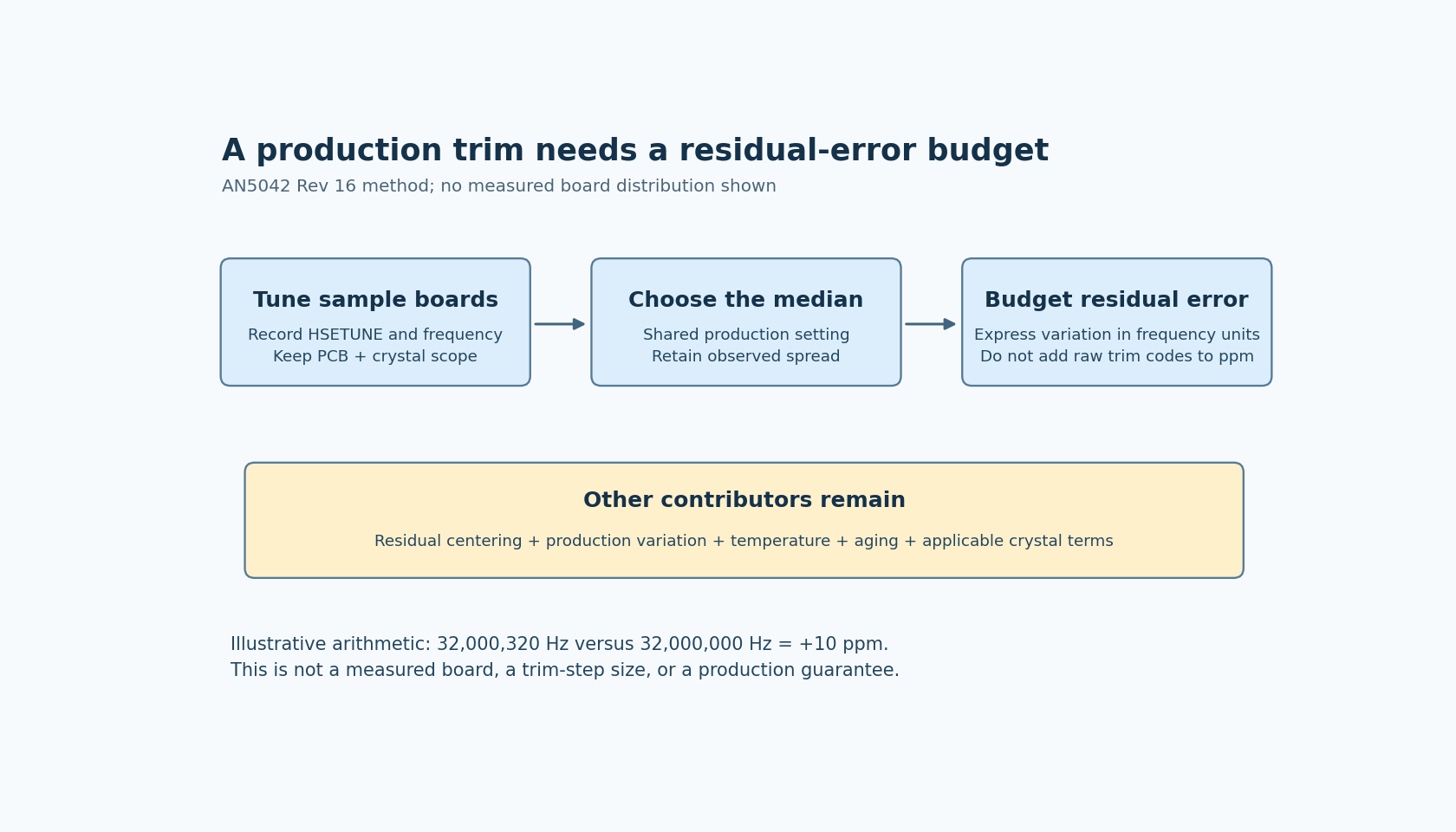
AN5042 section 1.9 proposes tuning a sample of boards, finding the median HSETUNE value and using that result for the other boards. It then uses the interval from that median to the observed maximum and minimum trim values to characterize the design's HSETUNE accuracy contribution.
The resulting potential frequency deviation must be added to the carrier-accuracy verification. Omitting that final step would turn the median into an unsupported guarantee that all boards behave like the median specimen.
The note suggests a sample of no more than a few dozen boards for the WB method. That is the documented engineering method, not a statistical assurance claim for every manufacturing process. Choose and justify qualification coverage for the actual crystal source, PCB implementation and production variation. A change in those inputs can invalidate the old sample's relevance.
Keep trim codes and frequency errors in different columns
HSETUNE is a capacitance selection, while the requirement concerns frequency. Do not add a raw trim-code spread directly to a ppm budget. Use the applicable tuning characterization and measurements to express its effect in the same frequency-error units as the other terms.
For an illustrative calculation only, a measured frequency of 32,000,320 Hz against a 32,000,000 Hz nominal differs by 320 Hz. Dividing by the nominal frequency and multiplying by one million gives a positive 10 ppm offset. This arithmetic does not imply that one HSETUNE step is always 10 ppm or that the example is an observed board.
Record the chosen trim code, measured frequency, reference accuracy, measurement conditions and residual error together. That preserves the distinction between a setting that can be reproduced and the evidence that justified it.
A useful budget has separate entries for residual centering, production trim variation, temperature, aging and the other applicable crystal terms. Define a consistent accounting method so a measured contributor is not also included a second time under a differently named tolerance.
Choose a measurement path the board actually exposes
AN5042 describes manual and software-assisted trimming methods, including outputting a clock for measurement. AN5378 also describes checking RF carrier centering with a spectrum analyzer. These are alternative observation routes with different fixture needs.
Its conducted RF example refers to a particular Nucleo board revision and component routing. Do not copy solder-component changes onto another revision without its schematic. Likewise, a clock-output pin used by a calibration example may already belong to the product's functional interface.
Plan that access before enclosure and fixture design are frozen. A correct numerical procedure is of little use if the production fixture cannot observe the chosen signal with adequate reference accuracy or repeatable loading.
Store the decision with its calibration scope
The release record should identify the PCB revision, crystal ordering code, sample conditions, selected median trim, residual spread and the resulting accuracy budget. Keep the firmware's applied setting associated with that record.
If the product stores per-device trim instead, that is a different manufacturing choice with its own measurement and storage process. AN5042's example of OTP or flash storage does not authorize an irreversible programming operation on a production unit.
No production-yield or RF-range improvement is claimed. The useful result is a fixed trim setting whose residual variation is visible, rather than a prototype number that silently consumes the product's clock-accuracy margin.