STM32G431 in 32 Pins: Design the ADC Reference Around the Bonding
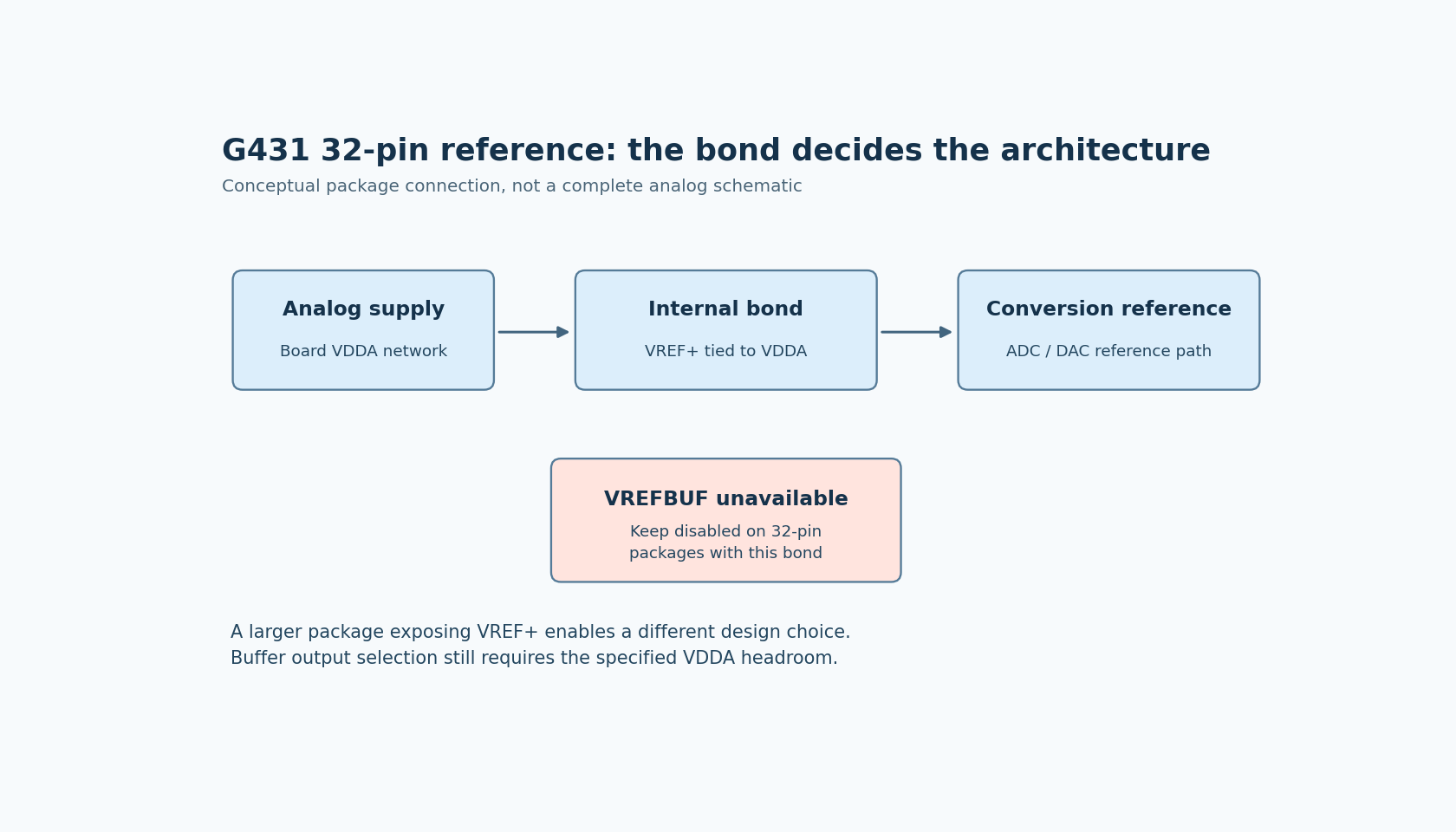
A 32-pin STM32G431 design cannot use VREFBUF merely because the product family lists an internal voltage-reference buffer. In this package class, VREF+ is bonded to VDDA, and ST says the buffer is unavailable and must remain disabled.
This restriction is explicit in AN5093 Rev 2, section 2.1. The G431 datasheet, DS12589 Rev 6, section 3.20 gives the general rule for packages with VREF+ double-bonded to VDDA. It is a package-selection constraint, not an ADC calibration option.
Begin with the bond connection
On a package exposing a separate VREF+ pin, the reference architecture can potentially use the internal buffer or a permitted external reference, subject to the electrical conditions. On the 32-pin arrangement discussed here, that separate board connection does not exist. The ADC reference is tied to the analog supply through the package bonding.
An initialization sequence cannot disconnect a physical bond. Nor does a successful write to a configuration field establish that the feature is supported in that package. The datasheet's package limitation remains the deciding evidence.
Record the full ordering code on the analog design sheet. “STM32G431” is too broad when the decision depends on whether a particular reference pin is available. This is especially important when a prototype uses a larger development-board package and the production board is later reduced to 32 pins.
Choose the measurement architecture that the package permits
For the 32-pin design, evaluate VDDA as the reference source used by the conversion path. The supply network therefore participates in the measurement architecture as well as powering analog circuitry. A nominal rail value in a schematic is not an accuracy specification.
If the product measures an absolute voltage, its conversion and calibration approach must account for the actual reference behavior. If it measures a ratio from a sensor excited by a related supply, determine whether the complete circuit preserves that relationship. These are design choices; the package restriction does not make either measurement strategy automatically accurate.
Alternatively, choose a package exposing the required reference connection, then recheck its pin table and electrical limits. That can be a cleaner design than trying to recover an unavailable reference path through increasingly complicated firmware.
Do not improvise an external reference connection to a pin that the selected package does not expose. Powering VDDA from a source is a supply-design decision with its own load and operating requirements, not the same operation as driving an independent reference input.
An exposed VREF+ pin is still not unconditional permission
For a supported package, AN5093 lists different analog-supply minima for the buffer's three nominal output selections: 2.4 V for 2.048 V, 2.8 V for 2.5 V, and 3.15 V for 2.9 V. These thresholds do not override the 32-pin prohibition.
They also make a useful schematic review example. A hypothetical design running VDDA at 3.0 V cannot justify selecting the 2.9 V buffer setting from the output voltage alone; the listed supply condition is not met. Moving to a package with VREF+ is necessary for that architecture but insufficient without the required supply conditions.
Use the datasheet's electrical characteristics for the final operating limits, output loading, accuracy and temperature conditions. The nominal setting is not a guaranteed system-level error bound. No reference accuracy or settling measurement is reported here.
Keep board configuration and firmware configuration together
Create a board-specific reference description that states whether VREF+ is separate or bonded, the intended analog supply range, and the permitted reference mode. Review the generated and handwritten initialization code against that description.
For the 32-pin target, the review should explicitly confirm that VREFBUF remains disabled. For another package, verify the actual reference source, required external components and initialization assumptions rather than inheriting the smaller board's configuration unchanged.
A useful proposed regression is a configuration-level check that rejects a board definition combining the 32-pin target with an enabled VREFBUF mode. That check is a project policy derived from the documentation; it is not a test performed here or a claim that every toolchain already enforces the restriction.
During later hardware qualification, observe the relevant analog supply and conversion behavior under the board's real loads and operating conditions. Keep that evidence separate from the simpler question of whether the requested reference architecture is supported at all.
The release decision is straightforward: approve the 32-pin package only when its bonded-reference architecture meets the measurement requirement, or select a package that exposes the needed reference path. Calibration can improve an implemented measurement system; it cannot supply a missing package connection.