STM32G474 DAC Sample-and-Hold: Budget Voltage Droop While the Output Is Tri-Stated
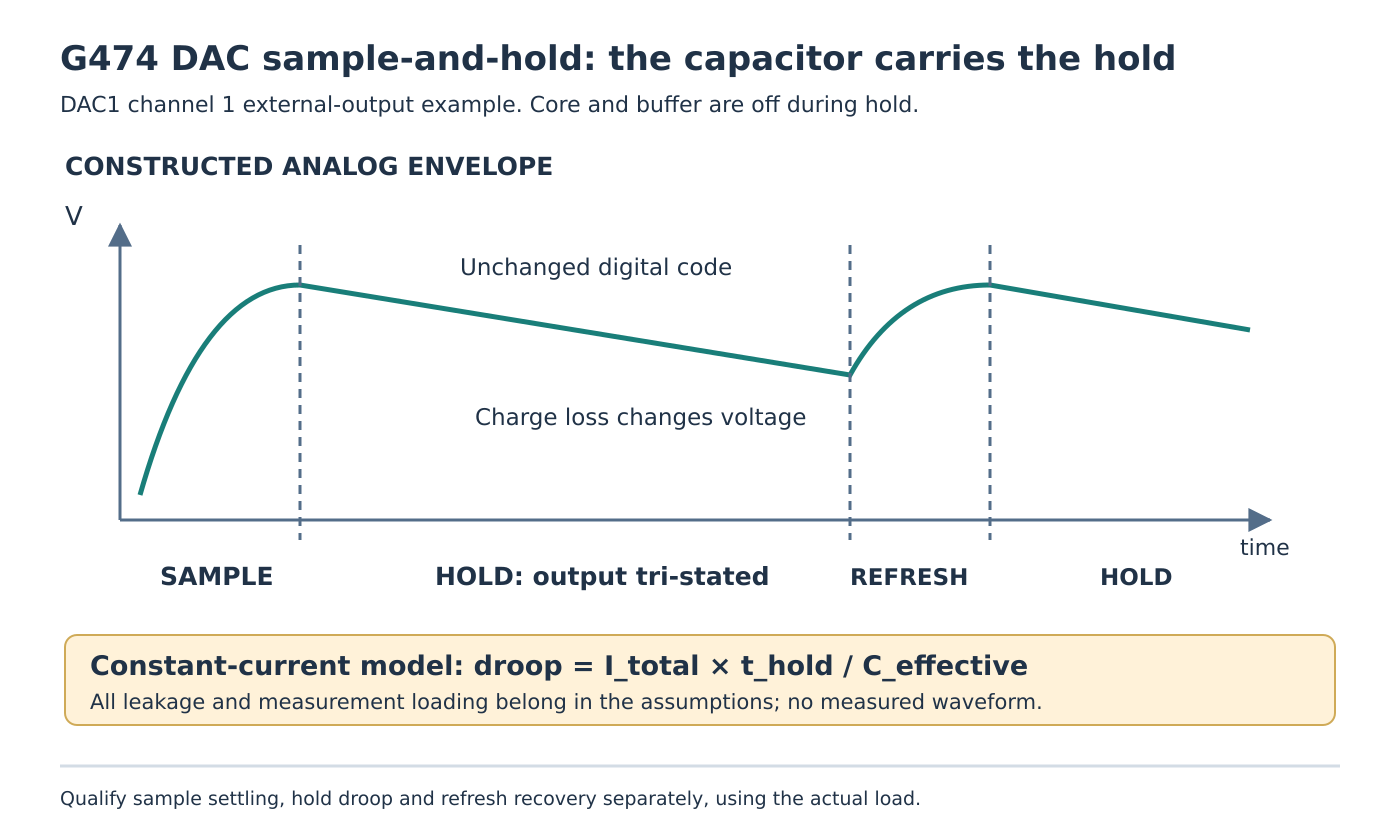
An unchanged DAC code does not guarantee an unchanged pin voltage during STM32G474 sample-and-hold operation. During the hold interval, the output is deliberately tri-stated. A capacitor retains the voltage while leakage and the attached circuit determine how far it moves before refresh.
This analysis uses DAC1 channel 1 as an inert external-output example, following RM0440 Rev 9, March 2025, section 22.4.12. DS12288 Rev 6 supplies the device-specific DAC context and electrical qualification boundary. No analog waveform, current consumption or board behavior was measured.
Treat hold as charge retention
The documented cycle has sample, hold and refresh phases. Sampling charges the selected capacitor toward the converted voltage. During hold, the core and buffer are off and the output is high impedance. Refresh restores charge before the next hold interval.
That changes the load assumption. A continuously driven output can supply current within its specified operating conditions; a held capacitor has a finite stored charge. An attached resistor, input leakage, board contamination or measurement instrument can contribute to its discharge. Firmware can preserve the exact digital value while the analog node still drifts.
Identify the actual channel, routing, buffer state, capacitor and load before calculating anything. The G474 has both external and internal DAC channels. Table 183 maps DAC1 channel 1 to PA4; DAC3 and DAC4 do not provide the same GPIO connection. Do not transfer an internal-capacitor assumption to an external pin without checking the selected mode.
Build a conditional droop budget
For a simplified constant discharge-current model, use:
droop = I_total * t_hold / C_effective
t_hold_limit = C_effective * allowed_droop / I_total
Here I_total is a justified bound on current removing charge from the node, not merely a typical MCU leakage number. C_effective should reflect the selected capacitor’s usable value under the relevant tolerances and operating conditions. A voltage-dependent resistive load may require a different model rather than a constant-current approximation.
For arithmetic only, assume C_effective = 10 nF, I_total = 50 nA and an allowed droop of 2 mV. The resulting hold limit is 0.4 ms. Holding for 1 ms under those same assumptions would lose 5 mV. These values are invented to show sensitivity; they are not G474 specifications, component recommendations or measured results.
Increasing capacitance can reduce droop for a fixed hold interval, but it also changes charging and refresh requirements. Treat it as a coupled design choice. A larger capacitor that never reaches the required voltage during the available sample phase does not solve the complete error budget.
Budget sample and refresh separately
Table 192 expresses sample and refresh timing using the capacitor, output resistance and buffer state. The manual’s accompanying numeric example is explicitly indicative and directs the reader to product data. Do not copy its leakage value across a different temperature range or claim its illustrated power reduction for another board.
Sampling must establish the required initial accuracy. Refresh must restore the charge lost during the permitted hold interval. Keep those errors separate from DAC offset, gain, reference error and downstream measurement error. An apparently small droop can coexist with a large initial settling error.
The phases use dac_hold_ck, selected from LSI or LSE, in addition to the AHB-domain clock. The low-speed clock must continue while sample-and-hold is enabled. A sleeping core therefore does not remove the clock requirement, and a nominal low-speed frequency should not be treated as an exact measured period.
Translate time into the correct field encoding
The channel-1 register descriptions give these different encodings:
sample time  = (TSAMPLE1 + 1) * low_speed_clock_period
hold time    = THOLD1 * low_speed_clock_period
refresh time = TREFRESH1 * low_speed_clock_period
Do not apply one blanket increment rule to all three fields. Sections 22.7.17–22.7.20 also define synchronization and write-state restrictions. Inspect those conditions before treating a software assignment as an effective timing change; an ignored write leaves the old operating assumption in place.
A change to DAC_DHRx interrupts the phase sequence and starts a new sample phase. Repeatedly rewriting a value while diagnosing hold behavior can therefore alter the behavior under observation. Sawtooth generation is explicitly unsupported in this mode and belongs to a different timing analysis.
Define a loading-aware bench check
A later test should use a disconnected, inert analog fixture and suitable high-impedance instrumentation. Include the instrument’s loading in the budget. Observe sampling, the worst permitted hold interval and refresh, then compare the measured voltage envelope with the predicted one under stated conditions.
Record the actual capacitor, load, reference, clock choice, register settings and temperature conditions. Keep the digital-code trace beside the analog trace so an update-triggered sample phase cannot be mistaken for periodic refresh. The acceptance claim should concern a qualified voltage envelope, not merely a code that stayed constant while the CPU slept.