STM32G474 External Memory: A 100-Pin Package Is Only the First Gate
Choosing an STM32G474 with at least 100 pins does not, by itself, establish that a proposed parallel memory can be wired to it. The family contains an FSMC, but package-specific restrictions further narrow the exposed banks and bus topology.
The decisive source is the package table and its footnotes in DS12288 Rev 6, followed by the FSMC description in RM0440 Rev 9. Read those before committing the processor, memory and PCB footprint as one purchasing decision.
Separate three questions that a feature list compresses
First, does the selected device line contain the controller? Second, does the package expose it? Third, does the exposed interface support the chosen memory's electrical and transaction topology?
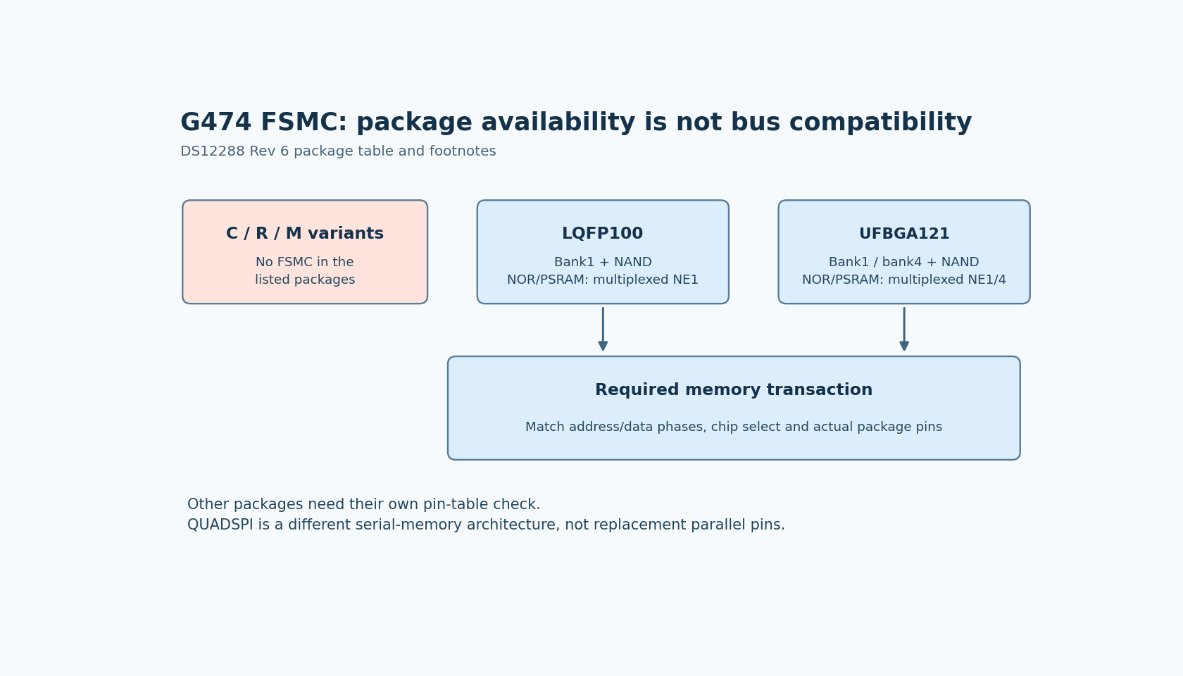
For G474, the datasheet limits FSMC availability to packages with 100 pins or more. Its feature table marks the C, R and M variants without that controller interface. A 64-pin G474RE therefore cannot be selected on the assumption that every G474 package supplies a parallel memory bus.
The next gate is less obvious. The LQFP100 footnote limits availability to bank1 and NAND. Bank1 can support only a multiplexed NOR/PSRAM arrangement using NE1. The UFBGA121 footnote identifies bank1, bank4 and NAND, with multiplexed NOR/PSRAM using NE1 and NE4.
Those restrictions are package-specific. They should not be generalized to every 100-pin or larger package, and the absence of one particular footnote elsewhere is not a substitute for checking the pin table.
Test the memory topology before calculating timing
Consider a hypothetical board proposal containing an LQFP100 G474 and a parallel memory with separate address and data buses. The relevant first question is whether the required signals and transaction mode exist in that package. It is premature to calculate read wait states while assuming an unrestricted nonmultiplexed bus.
A multiplexed interface uses the bus according to a different address/data sequence. The memory or its surrounding interface logic must support the intended sequence. Renaming processor pins in the schematic does not create the missing topology.
Build a signal-level compatibility sheet from the actual memory datasheet and MCU package table. Include address lines, data width, chip select, read/write strobes, address-latch requirements, clock or wait signals where needed, and supply compatibility. Mark each item with a specific MCU pin or a documented internal function.
This is also where alternate-function conflicts become visible. A memory interface that fits in isolation can still consume pins already reserved for a timer, communication port or board-level requirement. The solution may be a larger package, a different memory architecture or a board redesign; firmware cannot resolve two simultaneously required functions on one physical pin.
Do not substitute QUADSPI without revisiting the workload
G474 also offers a Quad-SPI interface. The datasheet describes indirect, status-polling and memory-mapped modes. This is a serial-memory interface, rather than another pin arrangement for the parallel FSMC bus.
A product that needs read-mostly external assets may be able to use a suitable serial flash. A product expecting ordinary writable scratch storage has a different requirement. Memory-mapped addressing alone does not make an external flash behave like RAM for arbitrary stores or erase-free updates.
Describe the workload in operations: reads, writes, erase operations, update granularity, concurrent use and startup availability. Then match those operations to the selected device and controller mode. Avoid making a bandwidth claim merely from the number of data lines; actual clocks, command phases, latency and competing traffic matter.
The same discipline applies to a parallel LCD connection. The datasheet describes an LCD interface supporting common controller-style protocols, but that does not establish compatibility with an arbitrary display panel. The panel's controller and required bus must be identified.
Make the schematic review produce a concrete artifact
The acceptance artifact should be a completed bus worksheet, not a screenshot of the product-page feature list. It should name the full MCU ordering code, package, memory part, selected bank, bus mode and every required signal assignment.
Resolve the package restrictions before selecting timing values. After that, derive timing from the actual memory requirements and MCU limits, and plan a board-level test covering reads, writes and any required mode changes. No such timing derivation or hardware test has been performed for this article.
One useful review challenge is to ask another engineer to reconstruct a single transaction from the worksheet. If the address phase, data phase or chip selection cannot be explained with the documented signals, the interface is not ready for layout.
The design gate is therefore stronger than “FSMC present.” It is “this exact package exposes a supported interface for this exact memory transaction.” Catching that distinction before routing is substantially easier than discovering it after the processor and memory footprints have been fixed.