STM32G431 PB8 CAN RX: Resolve the BOOT0 Input Before Releasing Reset
Connecting a CAN transceiver’s receive output to STM32G431 PB8 can affect the board before any FDCAN initialization executes. PB8 also serves as the physical BOOT0 input. When the boot configuration selects that input, its reset-time level participates in choosing the memory from which the processor starts.
The pin relationship comes from DS12589 Rev 6, Table 12, whose PB8-BOOT0 row includes FDCAN1_RX. The selection rules come from RM0440 Rev 9, section 2.6.1. Use the actual G431 ordering code and package column; no particular transceiver, factory option-byte state or board fault is assumed here.
Put the reset sample before the alternate-function write
An application can configure PB8 for FDCAN only after the processor has selected a boot path and reached that application. A later alternate-function write cannot determine an earlier boot sample. Likewise, a pull-down enabled by application code does not establish what PB8 looked like during reset.
RM0440 states that boot-selection values are latched on the fourth edge of the internal startup clock after reset release. Treat that as a hardware sequence, not a fixed microsecond delay inferred from the application’s eventual CPU clock. The required electrical condition must exist across the applicable sampling interval.
The manual also describes PB8’s reset-phase input behavior and its transition to analog mode. The later GPIO state is therefore separate evidence from the level that selected the boot destination. A register dump taken after successful initialization cannot reconstruct that earlier waveform by itself.
Decode the option-bit polarity explicitly
nSWBOOT0 = 1 selects the physical PB8/BOOT0 input. nSWBOOT0 = 0 selects the option-bit route using nBOOT0. The software route is inverted in the familiar-looking bit name: nBOOT0 = 1 selects main flash, rather than behaving like a high physical BOOT0 pin.
The following condensed form preserves all rows of the manual’s boot-selection table. “Either” means the input does not select the outcome in that row. The discussion concerns G431; dual-bank boot qualifications for other G4 devices must not be imported into it.
BOOT_LOCK |
nSWBOOT0 |
Selected input | nBOOT1 |
Selected boot area |
|---|---|---|---|---|
| 1 | Either | Either | Either | Main flash |
| 0 | 1 | PB8 = 0 |
Either | Main flash |
| 0 | 1 | PB8 = 1 |
0 | SRAM1 |
| 0 | 1 | PB8 = 1 |
1 | System memory |
| 0 | 0 | nBOOT0 = 1 |
Either | Main flash |
| 0 | 0 | nBOOT0 = 0 |
0 | SRAM1 |
| 0 | 0 | nBOOT0 = 0 |
1 | System memory |
The locked row is shown to keep the decode complete. It is not a recommendation to set BOOT_LOCK or change protection as a debugging shortcut. The electrical conflict below assumes BOOT_LOCK = 0 throughout.
Trace one hypothetical external-high condition
Suppose the actual configuration is nSWBOOT0 = 1 and nBOOT1 = 1, and a connected external driver holds PB8 at a valid high during the sample. The table selects system memory. Under the same option configuration, a valid low selects main flash.
This conditional result explains how wiring a receive signal can change startup even when the application image and CAN bit timing are unchanged. It does not establish that every transceiver drives high during power-up, that a particular bus state guarantees that level, or that system-memory code will expose a specific transport afterward.
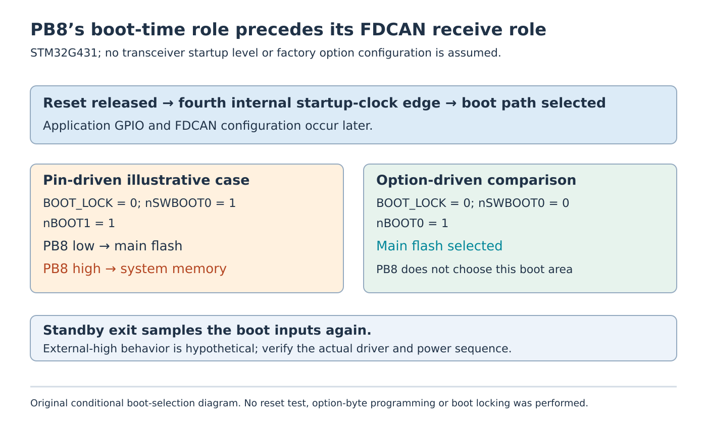
Now compare an already approved option-driven configuration with nSWBOOT0 = 0 and nBOOT0 = 1. That row selects main flash independently of PB8’s boot-selection level. This is a comparison of configurations, not an instruction to program option bytes. Recovery and manufacturing requirements determine which configuration is permissible.
Review the circuit during its earliest powered states
Record the transceiver or isolator part, its supplies, enable and standby controls, output behavior while unpowered or starting, and any external bias. An RX signal that behaves predictably after both devices initialize can still be unspecified during their power-sequencing gap.
Do not assume a stronger pull-down safely defeats an actively driven high output. Check permissible loading, logic thresholds, current and contention against the actual component documentation. No resistor value can be justified here without that circuit evidence.
Possible design reviews include retaining a compatible approved boot configuration, controlling the external driver’s reset-time behavior, or selecting another supported CAN route. Any alternative pin needs the exact package and alternate-function table. A route available on a different package is not evidence that it exists on this board.
Include Standby exit in the acceptance record
The manual says the boot inputs are sampled again on Standby exit. A circuit that establishes the right level only during cold power-up can therefore remain incomplete. Preserve the intended boot configuration during Standby and inspect the external driver’s state through that transition too.
A proposed isolated fixture observes reset, PB8 and relevant supplies, then verifies the selected boot destination through a supported observation method. Absence of an application heartbeat alone does not prove entry into ROM; reset loops, invalid firmware and other faults remain possible.
No reset experiment, option-byte change, boot lock or CAN transmission was performed. The deliverable is a boot-table decision tied to a reset-time electrical condition. Resolve that condition before diagnosing the later FDCAN configuration, because the affected application may never have started.