SPI Chip-Select Continuity: Keep Command and Data in the Transaction the Device Expects
Build one software transaction around the chip-select interval required by the peripheral. A command transfer followed by a data transfer can be correct when both belong to one SPI message, yet fail when issued as two independent operations that release chip select between them. Prove the intended grouping with a waveform capture, not just a successful API return.
Applicability: the concrete target here is Microchip 23LC1024 serial SRAM in ordinary single-bit SPI mode, using datasheet DS20005142E. Linux message semantics are checked against v6.12, with the official spidev documentation as the userspace reference. Dual/quad modes, other memories, and display-specific command pins are outside this example.
1. Extract the target’s transaction grammar
The Microchip datasheet defines a READ operation beginning with CS low, an eight-bit READ instruction, and a 24-bit address, followed by data. Raising CS terminates the read. In sequential mode, additional clocks read following addresses. These facts define the transaction boundary regardless of how many software buffers the controller uses.
Write a transaction worksheet before coding: device interface mode, opcode, address width, address byte order, payload length, bit order, clock polarity/phase, chip-select polarity, and required timing. Include the SRAM operating mode because byte, page, and sequential modes do not have the same address progression.
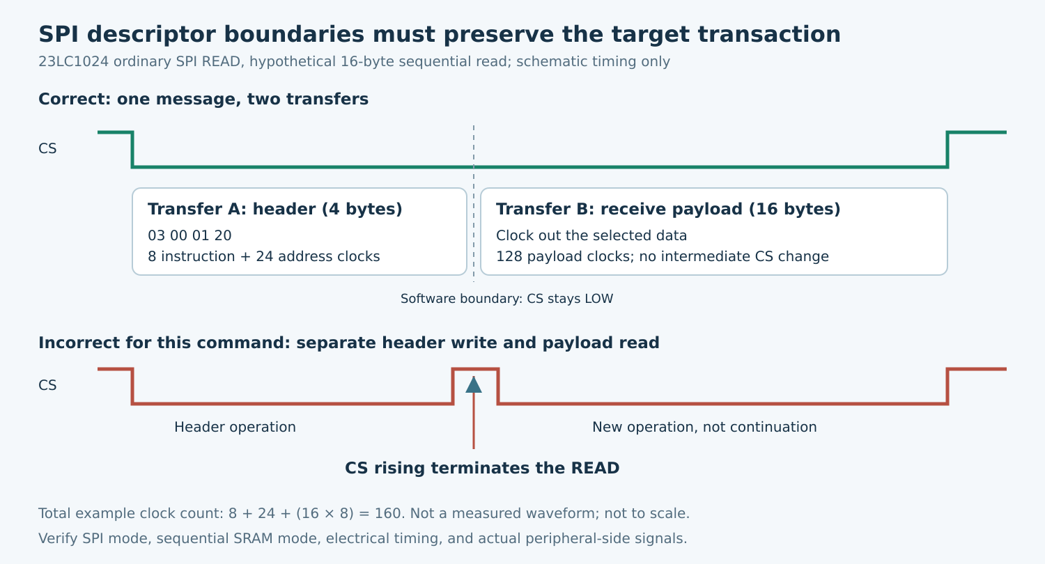
For a hypothetical diagnostic read, assume sequential mode has already been verified and request sixteen bytes beginning at address 0x000120. The ordinary SPI header is four bytes: 0x03, 0x00, 0x01, 0x20. The payload requires sixteen additional clocked bytes. This is an illustrative transaction specification; no SRAM contents or measured result is claimed.
2. Map protocol phases to one message
A natural Linux representation uses two transfers in one message. The first sends the four-byte header; the second receives sixteen bytes while the controller supplies clocks. Keep eight-bit word framing and the selected SPI settings consistent across both phases. The descriptor boundary is a memory and scheduling description, not permission to terminate the device command.
The Linux v6.12 SPI header documents that CS normally remains active across transfers in a message. An intermediate transfer with cs_change set requests a brief inactive interval. For this read, use no intermediate CS change, and ordinarily let CS become inactive after the final transfer.
The same header defines message atomicity as excluding another SPI message from the bus until the sequence finishes. That is bus ownership, not a promise of continuously running SCK. A controller can pause between transfer segments while CS remains active. Review any target clock-gap restrictions separately from chip-select continuity.
3. Recognize the userspace split-operation trap
The Linux spidev API documentation explicitly states that separate read() and write() operations deactivate chip select between them. A write of the SRAM header followed by a read of the payload therefore does not preserve the required selection interval. The second operation is no longer a continuation of that READ command.
SPI_IOC_MESSAGE(2) can describe the two phases as a composite operation. Start from zero-initialized descriptors, populate only the intended fields, and preserve the requested transfer lengths. If using a receive-only second descriptor, verify the controller’s transmitted fill behavior and whether the target cares about incoming bits during readout.
Do not solve the split by manually driving a CS GPIO from an unrelated thread while the SPI driver also owns the bus. That creates a second ownership mechanism and can conflict with another device’s transaction. If the hardware cannot express the required message, address that through a supported controller or driver design rather than an unsynchronized userspace workaround.
4. Review every source of an unwanted CS edge
Audit helper functions that submit their own message per buffer. A function named read_register may hide one header write and another payload read. Inspect the actual submission path, including adapter libraries, not just the top-level call that appears to describe one logical read.
Check every descriptor’s cs_change value, zero-initialization, and final-transfer behavior. The v6.12 documentation gives special semantics to cs_change on a final transfer; it is not a general-purpose guarantee that two independent messages will remain one uninterrupted peripheral transaction. Keep the complete command in one message when its length and response structure allow it.
Also review controller maximum transfer and message sizes, hardware-managed versus GPIO-managed CS, runtime power transitions, and driver-specific chunking. Larger buffers may exercise a different path from a small diagnostic read. A driver that splits memory work must still preserve the peripheral’s visible protocol boundaries.
5. Correlate descriptors with the physical waveform
Capture CS, SCK, MOSI, and MISO at the peripheral side of any isolator or level shifter. Record the driver version, configured rate, board revision, and test request identifier with the capture. Confirm analyzer polarity, phase, and bit-order settings against the target, then inspect raw edges when decoded bytes look inconsistent.
- Selection: CS becomes active before the header and stays active through the final payload bit.
- Header: decoded bytes match the requested opcode and address. Verify all address bytes, not just the first command byte.
- Boundary: there is no inactive CS pulse between the fourth header byte and the first payload byte. Inspect at sufficient time resolution to see a narrow glitch.
- Clock count: this illustrative request needs 160 clocks: 32 for instruction/address and 128 for sixteen payload bytes.
- Completion: CS becomes inactive only after the final data transfer and the device’s required hold timing.
The clock count is arithmetic from this example’s fields, not a measured trace. Select rate and setup/hold margins from the datasheet’s applicable electrical conditions and the board path. Do not copy a headline maximum frequency without checking voltage, loading, and controller behavior.
6. Test boundaries that a short read misses
Use a disposable SRAM test range with known data written through a separately qualified transaction. Check several start addresses and lengths, including values around the controller’s internal chunk boundary. Keep reads within the intended array region unless wraparound is the specific test. A repeating fill pattern can hide address errors, so use distinguishable neighboring values.
Repeat with other devices active on the same SPI bus. The complete message should retain its transaction boundaries under contention. Test a deliberately split header/data request as a controlled negative case, but do not assume a particular returned byte pattern: target state and the second operation’s clocks determine the result.
If CS remains continuous but data is wrong, examine opcode/address encoding, operating mode, sampling phase, clock rate, and the prepared memory contents. If CS rises precisely at a descriptor or helper boundary, inspect message construction before changing electrical parameters. These observations narrow the next investigation without proving a cause by themselves.
The acceptance package is the target transaction worksheet, software descriptor map, and matched waveform captures for normal and boundary cases. No Linux SPI operation or SRAM test was executed for this article. Controller-specific behavior and physical timing remain qualification work for the selected board.