STM32G431 Internal OPAMP: Decide Whether It Can Replace the External Amplifier
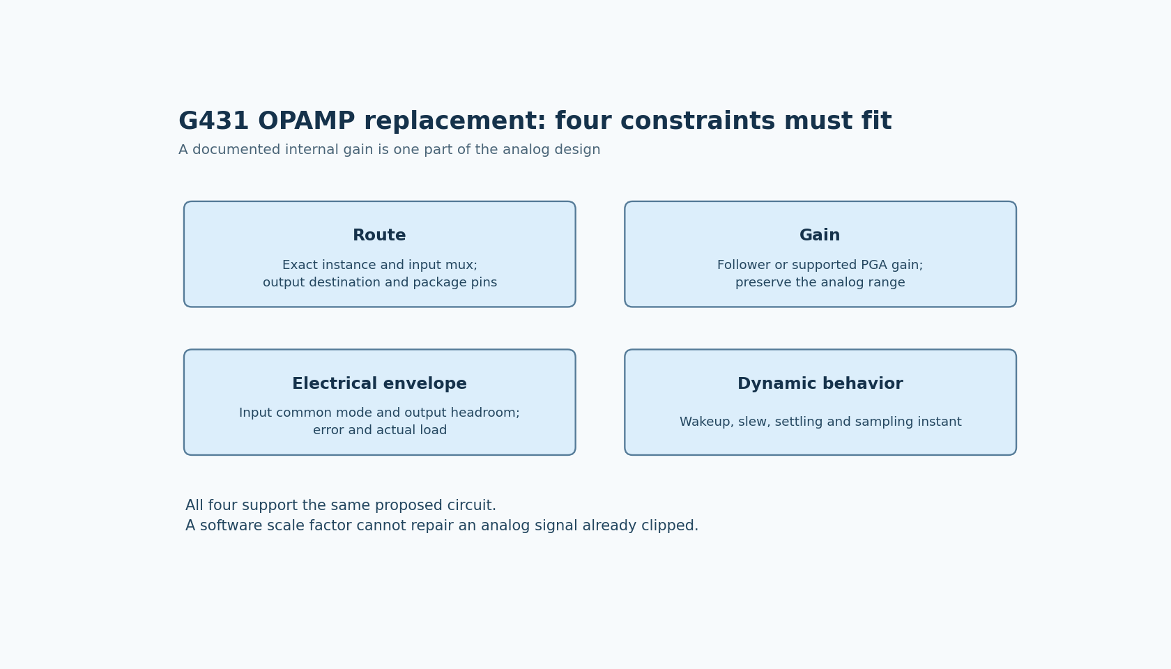
Replacing an external amplifier with an STM32G431 OPAMP is a signal-path decision, not a part-count decision. The internal block must accept the required input, provide an available gain, reach the required output under its actual load and connect to the intended ADC or pin.
Use AN5306 Rev 1 to understand the internal multiplexers and feedback choices. Use DS12589 Rev 6, Table 74 for G431 electrical conditions. The application note's approximate performance summary is not a substitute for the datasheet's conditional limits.
Draw the proposed replacement as an actual circuit
Start with the external circuit's job: input range and common mode, gain, bandwidth, offset allowance, source impedance, output load and startup behavior. Include any protection or filtering provided by components that the cost-down proposal intends to remove.
Then trace the internal route using the exact OPAMP instance and package. AN5306 describes separate input multiplexers, a connection to internal feedback for PGA operation and a follower connection. A peripheral called OPAMP does not imply arbitrary routing between every package pin and every ADC channel.
The G4 reference manual supplies the instance-specific interconnect and control fields. Record the selected positive input, negative-input configuration, output destination and any pin conflict. An unresolved connection is a failed replacement proposal even when the nominal gain is attractive.
Match the gain without inventing intermediate settings
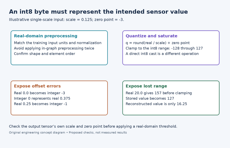
The documented non-inverting PGA gains are 2, 4, 8, 16, 32 and 64. Follower operation is a separate connection. A requirement for a gain of 10 therefore cannot be met by selecting an undocumented internal setting.
Possible redesigns include another supported gain with a changed input range, external feedback where the selected configuration permits it, or retaining the external amplifier. Each changes the circuit's error and dynamic-range budget. Dividing the ADC result by a different software constant does not prevent analog clipping that happened before conversion.
The datasheet also assigns different gain-error conditions to different gains. In Table 74, higher PGA gains use different output-range margins and accuracy limits from several lower-gain cases. Read the row for the selected gain instead of applying one headline percentage to every configuration.
This is particularly important for a small signal requiring large gain. Input offset and gain error can become a substantial part of the useful output range even when the ADC has many available codes.
Separate input rail range from usable output range
Table 74 gives the OPAMP analog-supply range as 2.0 V to 3.6 V and the common-mode input range as zero to VDDA. That input statement does not promise linear output operation at either rail for every load and gain.
The same table specifies output saturation and gain characteristics under stated loading and output-range conditions. A sensor signal can therefore be legal at the input while its amplified output violates the application's linearity or headroom requirement.
For an illustrative feasibility check, calculate the nominal amplified minimum and maximum, then add the relevant error allowances and compare with the specified usable output range. Keep the ADC's permitted input range in the same worksheet. Passing only the amplifier-input check leaves half the path unqualified.
Do not treat the internal amplifier as a general-purpose load driver. External capacitance, wiring and resistive load must fit the documented conditions. A direct internal ADC path and a connector-driving output are different workloads.
Check dynamics at the selected operating mode
The datasheet distinguishes normal and high-speed slew-rate characteristics and gives wakeup conditions. AN5306 explains the available operating configurations, but its typical bandwidth summary cannot establish the settling time of a specific large-signal step through the chosen gain and load.
Define when the ADC is allowed to sample after enabling the amplifier or changing the input. Include wakeup, signal settling and any relevant multiplexer changes. An ADC result that is numerically within range can still represent an unsettled amplifier output.
A later bench comparison should use the actual source impedance and load, the smallest and largest intended signals, and the required operating conditions. Measure the complete transfer and settling behavior rather than comparing one room-temperature DC point. No amplifier or ADC measurement was performed here.
Keep the external part when its function is still needed
The replacement is justified only if routing, gain, electrical limits and dynamics all meet the product requirement. An external amplifier may still be required for precision, drive, protection or a topology the internal block does not provide.
Document which external components remain and why. A successful internal-amplifier demonstration does not establish that the original front end's protection and filtering can also be removed. The useful outcome is a supported circuit substitution with explicit limits, rather than a smaller bill of materials that silently changes what the measurement means.