STM32G474 Differential ADC Inputs: Check Common Mode Before Interpreting the Signed Signal
A small voltage difference between two STM32G474 ADC inputs is not sufficient to make a valid differential measurement. Both absolute pin voltages and their common mode must fit the differential front end. Two inputs can remain between ground and the positive reference while violating the common-mode condition.
The concrete example here is ADC1 channel 1 on an STM32G474RE LQFP64: PA0 supplies the positive input, and the paired PA1 path supplies the negative input. The source baseline is DS12288 Rev 6, Table 66 and RM0440 Rev 9, sections 21.4.4, 21.4.7 and 21.4.8. Other channels require their own connectivity check.
Calculate common mode before interpreting the difference
For the proposed sensor connection, calculate two quantities from the voltages at the ADC pins:
Vdiff = VINP - VINN
Vcm   = (VINP + VINN) / 2
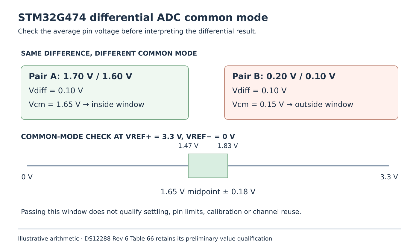
Table 66 gives the differential input common-mode window as the reference midpoint plus or minus 0.18 V. The table explicitly describes its parameters, unless otherwise specified, as preliminary values derived under the conditions associated with Table 17. Preserve that qualification and the table’s footnotes when turning it into a product requirement.
With an illustrative VREF+ = 3.3 V and VREF- = 0 V, the arithmetic window is 1.47 V to 1.83 V. Consider two pairs:
- 1.70 V and 1.60 V produce a difference of 0.10 V and a common mode of 1.65 V.
- 0.20 V and 0.10 V produce the same difference, but their common mode is 0.15 V.
Only the first pair passes this particular common-mode check. Neither calculation proves complete ADC accuracy. The second pair cannot be made admissible by subtracting an offset after conversion. Its failure is an analog operating-condition problem that exists before software sees a result.
Budget both pins over the entire signal excursion
Treat the midpoint as a controlled front-end quantity. For a balanced signal, the proposed pin voltages are Vcm + Vdiff/2 and Vcm - Vdiff/2. Check both against the pin and conversion limits at minimum and maximum signal, reference tolerance, amplifier offset and expected common-mode movement.
A negative differential voltage means that the positive input is lower than the negative input. It does not authorize either physical pin to go below its permitted range. Likewise, centering the nominal signal correctly does not qualify an amplifier whose output clips during startup or whose two outputs settle at different times.
If the sensor naturally operates near ground, decide whether an appropriate level-shifting or differential driver stage is required, or whether another acquisition topology better matches it. This is a circuit decision. Increasing digital filtering or calibration samples cannot supply missing analog headroom.
Reserve the negative-input channel in the scan plan
RM0440’s ADC1 connectivity diagram connects channel 1’s negative input to the channel 2 input path. For the selected G474 example, the datasheet identifies PA0 as ADC12_IN1 and PA1 as ADC12_IN2. Do not infer that every desired pair of pins can be selected as an arbitrary differential input.
The manual warns that a channel consumed as another channel’s negative input must not also be configured for conversion, whether single-ended or differential. Shared paths can also affect another ADC instance; consult the exact connectivity diagram rather than allocating each ADC independently. The documented interleaved master/slave exception is specific, not general permission to reuse the pin.
Review regular and injected sequences together. A background diagnostic that adds the consumed channel to an injected sequence can invalidate an otherwise correct regular scan.
Configure and decode the differential mode deliberately
Write the DIFSEL selection while the ADC is disabled, as required by section 21.4.7. Use the differential calibration selection, ADCALDIF = 1, for the differential calibration procedure, and wait for completion. Single-ended and differential calibration factors are distinct.
For the unshifted 12-bit transfer described in that section, zero differential input maps to 0x800; the negative and positive endpoints map to 0x000 and 0xFFF. A raw result is therefore not already a signed two’s-complement sample. For this configuration, subtracting 2048 in a sufficiently wide signed type centers the code. Revisit the interpretation when resolution, alignment, offsets or oversampling configuration changes.
Qualify the electrical condition independently of the code
A useful proposed fixture holds common mode near the reference midpoint while applying small positive, zero and negative differences. Record both pin voltages, reference voltage and raw ADC codes. Then check the permitted common-mode excursion using the actual front end and acquisition timing, without exceeding device limits.
Keep source impedance and sampling time in the same review; DS12288 Table 67 makes their relationship explicit. Correct common mode does not remove settling, reference or concurrent-ADC limitations.
No voltage sweep or ADC measurement was performed here. The release question is whether the full signal envelope, channel allocation and result encoding satisfy the selected differential configuration. A plausible signed number alone answers none of those checks.