STM32H750 SDRAM Retention: Enter Self-Refresh Before Removing the Memory Clock
Selecting SDRAM power-down does not transfer refresh responsibility to the memory chip. On STM32H750, stopping the controller’s clock after that choice can remove the refresh operations the data still needs. Self-refresh is the relevant mode when the SDRAM must retain data without external clocking.
This review uses RM0433 Rev 9 and keeps the qualified memory frequency and timing configuration unchanged before and after the retention interval. It establishes the SDRAM-side conditions; it is not a complete MCU Stop-mode recipe or permission to gate arbitrary clocks.
Identify who performs refresh in each mode
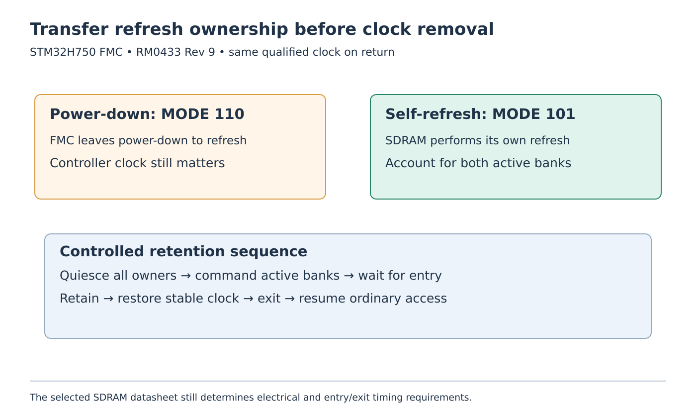
RM0433 section 22.9.4 distinguishes self-refresh, where the SDRAM performs refresh itself, from power-down, where the FMC controller still supplies refresh. In power-down, the controller periodically exits the mode, refreshes the memory and returns it to power-down.
The command distinction is explicit: FMC_SDCMR.MODE = 101 selects self-refresh, while MODE = 110 selects power-down. Target bits CTB1 and CTB2 select the affected SDRAM banks. A variable called “sleep mode” in application code is insufficient evidence; inspect the command actually issued and its bank selection.
Make a bank inventory before altering the low-power path. Record which bank is initialized, which external device occupies it, and which timing qualification applies. If two devices are active, placing only one in self-refresh does not establish the conditions for stopping the shared memory clock.
Quiesce memory users before commanding retention
List every source of SDRAM access: instruction fetch, stack, interrupt handlers, data structures, DMA and display or other bus masters. Arrange the transition code and required working storage so they do not depend on the SDRAM being placed into retention. Merely putting the CPU to sleep does not show that every other master stopped accessing it.
The reference manual states that selecting an SDRAM device triggers an exit from self-refresh, after which it remains in Normal mode. An unnoticed access can therefore change the retention state before the intended clock removal. Treat quiescence as an owned part of the transition, with a defined point at which new accesses are prevented.
Do not use a live production framebuffer or active control data as the first retention experiment. Reserve an inert test region and use a recoverable development setup. This lets the test examine retention without making an incomplete memory-mode sequence responsible for equipment behavior.
Wait for entry rather than assuming the write completed it
For self-refresh entry, FMC issues precharge-all and drains pending writes before activating the mode. The documented BUSY interval includes the minimum self-refresh entry period associated with TRAS. Follow the applicable command-completion procedure instead of treating a completed register write as proof that the external memory is already retaining data autonomously.
The manual’s clock-stop condition accounts for both banks: self-refresh must cover both active devices, with the documented exception for an unactivated, uninitialized bank. Keep an unused bank’s target bit clear when issuing a command for the sole used bank. A physically absent memory and an initialized second bank are not interchangeable software states.
Retain the selected SDRAM datasheet’s electrical requirements and timing values with this sequence. The controller manual defines the mechanism, but it does not select a universal tRAS or tXSR for an unspecified memory part.
Restore the same qualified clock before normal access
Design the wake path around a stable restored memory clock and the selected device’s exit requirements. The documented Normal-mode command uses MODE = 000 with the target-bank bits. Review the programmed exit delay and keep ordinary traffic excluded until the controlled transition is complete.
This is deliberately not a dynamic-frequency-change recipe. RM0433 also says not to reprogram FMC_SDRTR after initialization. Do not turn retention work into an improvised refresh-counter adjustment, or copy a universal COUNT expression without reconciling the part, clock and applicable documentation.
Preserve evidence from a bounded retention check
Propose known nonuniform patterns in the inert region, a recorded bank-command sequence, a defined retention interval and a controlled return to the original clock configuration. After wake, compare the retained region while accounting separately for any software caching that could conceal the external memory contents.
Repeat with the intended access owners disabled and verify that none resumes before memory readiness. Include the two-bank configuration when the product uses it. No such target test was executed here; retention duration and electrical margins remain qualification results to obtain, not promises from this source review. The first acceptance question is concrete: after the external clock disappears, which component is still responsible for refreshing each active SDRAM device?