HART Input Filtering: Do Not Quiet the ADC by Shorting the Communication Signal
An analog input becomes less noisy after a capacitor is added across its current-sense resistor. The displayed process value looks better, but HART communication becomes unreliable. Both observations can be electrically consistent. A component that removes the unwanted AC content from the ADC reading can also remove the AC voltage the modem needs if it is placed at the shared input rather than in the measurement branch.
The architectural references are Analog Devices technical article TA13144-0-4/15, “Flexible Bandwidth 4 mA to 20 mA Current Input with Easy HART Compatibility,” and circuit note CN-0414 Revision 0. The calculations below use an explicitly simplified resistor-capacitor model. They are not simulations of either reference circuit, measurements, or a claim of HART physical-layer compliance.
Split the two receive objectives
A HART-enabled current input has two different observations to preserve. The process-measurement path should recover the analog value while rejecting communication ripple. The modem path should recover the communication while rejecting the slow analog component and unwanted interference. Applying the same low-pass behavior to both paths defeats that separation.
The ADI technical article illustrates AC coupling to the modem and separate filtering before analog conversion. Its two alternatives distribute analog and digital filtering differently. CN-0414 shows a dedicated modem input network connected to the current-input terminal. These are useful architectural examples, not permission to transplant one component into an otherwise unrelated input card.
For a design review, mark the exact point where the two signal paths separate. Then identify every component that loads the shared node before that split: protection devices, capacitors, resistors, multiplexers, and any connected diagnostic equipment. A capacitor on that list needs an AC impedance assessment even when it has almost no effect on the static current reading.
A DC resistance is not the AC impedance
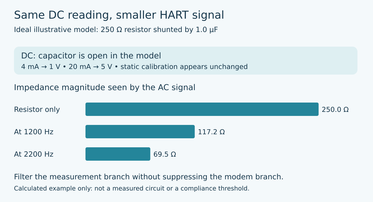
Consider a hypothetical ideal current source feeding a 250 Ω resistor. Add a 1.0 µF capacitor directly in parallel with that resistor. At DC, the capacitor is open in this ideal model, so the resistance still converts 4 mA to 1 V and 20 mA to 5 V. A static endpoint calibration can therefore appear unchanged.
At frequency f, the magnitude of the parallel impedance is R divided by the square root of 1 + (2πfRC)². With the chosen values, RC is 250 µs. At 1200 Hz the impedance magnitude is approximately 117.2 Ω; at 2200 Hz it is approximately 69.5 Ω. Relative to the resistor alone, the resulting voltage amplitudes are about 0.469 and 0.278 of their original values.
For a hypothetical injected 1.0 mA peak-to-peak sinusoidal current, the resistor alone would produce 250 mV peak-to-peak. The parallel capacitor reduces that result to approximately 117 mV at 1200 Hz and 69.5 mV at 2200 Hz. These are standalone small-signal calculations, not acceptance thresholds. The deliberately simple example demonstrates why the DC calibration and the digital channel can disagree after one apparently harmless filtering change.
A real installation requires more than this two-component model. Cable capacitance, protection networks, other loop devices, source impedance, and the modem coupling network affect the actual transfer function. The model’s role is to expose the missing question: what impedance does the communication signal see at the terminal?
Filter the measurement path without assuming isolation
The obvious design direction is to put the required measurement filtering in its own branch while preserving the modem’s intended signal path. However, drawing two branches does not make them electrically independent. A filter input can still load the shared node, and a buffer has finite bandwidth, input impedance, protection structures, and supply constraints.
Review the complete circuit against the selected components’ documentation. Evaluate terminal impedance and modem signal levels, then assess analog rejection and settling. Do not solve an ADC problem by assigning every capacitor to “EMC” and excluding it from the communication analysis. Component function labels describe intent; impedance determines what the circuit actually does.
Digital filtering can provide additional flexibility, but it does not restore a signal already removed before the modem. It also changes the measurement path’s bandwidth and settling behavior. Record the ADC configuration with the electrical design so that a later firmware change does not silently alter the analog response promised during integration.
A tone check is useful but incomplete
The ADI technical article cautions that a complete modulated message contains spectral energy beyond the two nominal signaling frequencies. Consequently, demonstrating rejection at two individual tones is not sufficient to establish analog accuracy during real communication. Likewise, observing a carrier at the modem input does not prove reliable decoding of messages under the intended operating conditions.
Build the proposed verification around both channels. First, establish the static analog transfer with communication silent. Next, compare the process reading with representative valid communication active while keeping the underlying analog condition fixed. Then apply permitted analog changes and check the modem path at the same time. Preserve the distinction between a recovered mean value, transient error, settling time, and communication success.
For a capacitor-change investigation, compare the same installation before and after the change using a controlled test setup. Record the shared terminal waveform and the modem-side observation alongside the ADC result. Use measurement equipment and grounding appropriate to the loop’s voltage and isolation. A probe or adapter that introduces an additional return path can change the circuit being diagnosed.
Release two separate acceptance records
The analog record should state range, permitted error, filter configuration, settling requirement, and the communication conditions included in the evaluation. The modem record should identify the interface circuit and the relevant physical-layer and interoperability checks. Neither record substitutes for the other.
The resulting engineering decision is more precise than “the capacitor helps” or “HART dislikes filtering.” Filtering is necessary, but its location and loading determine which signal it removes. Preserve the shared terminal’s communication behavior, then reject communication content in the process-measurement branch where rejection is actually wanted.
Primary references
Analog Devices CN-0414 Revision 0, HART Input and Output Circuit, printed page 5.