Industrial pH Inputs: Budget Leakage Before Adding ADC Resolution
A glass pH electrode can produce a perfectly ordinary-looking voltage while behaving nothing like a low-impedance voltage source. A gateway that reads a bench calibrator accurately may load the real electrode enough to introduce a meaningful error. More ADC bits will not repair that loading, and averaging will not remove a steady leakage current.
For this interface, the useful starting point is the current allowed to enter or leave the sensitive input. That current budget includes the amplifier, protection components, connector, PCB surface, and any attached test equipment. The advertised input-bias current of one component is only one part of the complete path.
Turn the error allowance into a current allowance
Texas Instruments’ AN-1852 describes glass-electrode source resistance typically ranging from 10 MΩ to 1000 MΩ. It also gives the ideal sensitivity at 25°C as 59.16 mV per pH unit. The relevant resistance depends on the actual electrode and conditions; the upper end of that range should not be silently replaced by a convenient bench-source impedance.
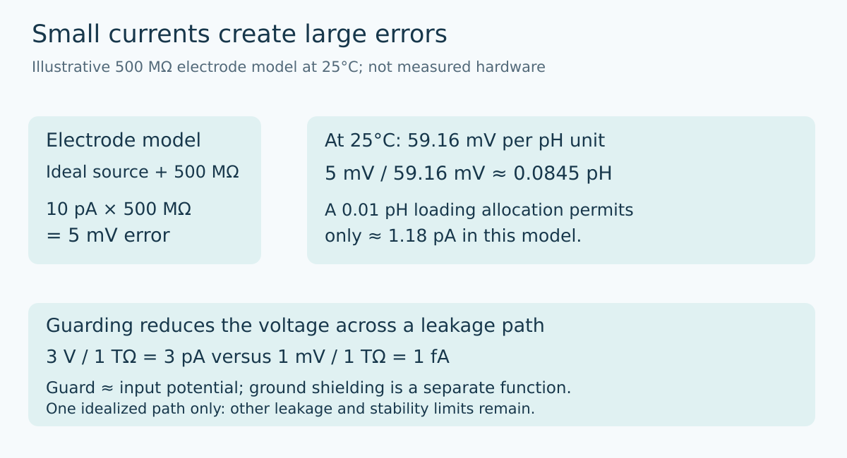
Consider an illustrative allocation of 0.01 pH for electronics loading error at 25°C. With the ideal sensitivity, that corresponds to 0.5916 mV. If the electrode is modeled as an ideal voltage source in series with 500 MΩ, the allowable net input current for that allocation is 0.5916 mV divided by 500 MΩ, or approximately 1.18 pA.
A 10 pA leakage current through the same modeled source resistance creates 5 mV, equivalent to roughly 0.0845 pH at the stated sensitivity. Those values are calculations, not measured electrode performance. They illustrate why a current too small to notice in many interfaces can dominate a high-impedance measurement.
This simple resistance model is useful for an electronics budget, but it does not reproduce electrode electrochemistry, response time, or all frequency-dependent behavior. Keep that boundary explicit when choosing a simulator or interpreting a test.
The leakage path can bypass the amplifier specification
Imagine a high-impedance input near a conductor whose voltage differs by 3 V. A hypothetical 1 TΩ parasitic surface path carries 3 pA. Even that apparently enormous resistance exceeds the illustrative 1.18 pA allocation. Surface contamination or a connector path need not resemble an obvious short to matter.
Conversely, a low-impedance calibrator can supply that leakage current while maintaining nearly the expected voltage. Passing a direct voltage-source check therefore does not establish acceptable loading of a glass electrode. The source resistance is part of the test condition, not an incidental fixture detail.
List the possible paths before choosing remedies. Include amplifier bias over the required temperature range, protection-device leakage at the actual applied voltage, connector insulation, board surface leakage, and instrumentation loading. Do not combine favorable room-temperature typical values into a guaranteed system limit.
A guard is not just another ground trace
The LMP7721 datasheet describes a guard as a low-impedance conductor surrounding the sensitive input and held close to that input’s potential. The purpose is to reduce the voltage across a leakage path. Grounding an adjacent conductor does not achieve the same result when the input itself is not at ground potential.
For example, if a hypothetical 1 TΩ path terminates at a guard only 1 mV away from the input potential, its current is 1 fA rather than the 3 pA produced by the earlier 3 V difference. This is an idealized comparison of one path. It does not prove that all contamination, connector, or protection leakage has been intercepted.
Guard drive also has electrical requirements. Its source must handle the implemented capacitive load without introducing instability or excessive noise. Follow the chosen amplifier’s supported guard arrangement rather than connecting an arbitrary output to every available copper area. The LMP7721 guidance distinguishes guarding from external shielding; the guard is not a substitute for an appropriate ground shield.
Preserve the sensitive region through assembly
A clean schematic can become a poor high-impedance input after layout or rework. The LMP7721 datasheet calls for guarding the input connections on both PCB sides and gives specific solder-mask and cleaning guidance. Apply the actual component’s recommendations and manufacturing process rather than copying only a top-layer ring from an example drawing.
Review the connector pins, vias, exposed test points, and paths under components. A through-hole connection can expose the sensitive node on the opposite board surface. A production fixture that contacts the node can introduce a new leakage route even if the released product layout is sound.
The practical release question is whether the assembly process preserves the intended insulation and guarding. A design review should identify which cleaning, handling, and inspection steps are necessary for this input, and how rework returns the assembly to that condition. This is an engineering process requirement, not a cleanliness certification claim.
Qualify the buffer without mistaking it for the electrode
Begin with a supported input voltage and the intended reference-electrode or common-mode arrangement. Compare the buffer result with a low-impedance source, then with an appropriate high-resistance source model that stays within all component limits. Observe whether the change agrees with the proposed leakage-current budget.
Use instrumentation suitable for that impedance level. Attaching an ordinary meter directly to the sensitive node can load it more than the circuit being evaluated. Measurement equipment should be part of the documented model rather than an invisible observer.
Keep electrode calibration and electronics loading separate. Calibration can characterize offset and sensitivity for a particular electrode under defined conditions. It does not demonstrate that a gateway maintains negligible leakage after temperature, humidity, contamination, or connector changes. Nor does temperature compensation of the ideal electrode slope automatically correct every solution-dependent pH change.
The resulting interface contract should state supported electrode conditions, allowable loading, input range, guard arrangement, and the scope of calibration. A defensible pH channel starts by preserving the electrode voltage, then converts it. Resolution matters only after that first condition is met.
Primary references and trend scope
Texas Instruments AN-1852, SNOA529A, April 2013 revision provides the electrode and bias-current foundation. Texas Instruments LMP7721 datasheet, SNOSAW6E, sections 8.1 and 10 provides guarding and layout guidance. All numerical leakage examples above are hypothetical.
The preserved Google Trends RISING row “industrial iot solutions,+110%,” worldwide, all categories, web search, July 19–October 19, 2026 supports the parent topic only. It is not evidence of title-specific or pH-sensor search growth.