ADC Source Impedance and Acquisition Time: Explain a Reading That Improves When Sampling Slows
A reading that improves when sampling slows suggests a timing-dependent error, but it does not identify which timing interval is responsible. Separate the ADC’s acquisition window from the period between conversions, then vary each independently. This distinguishes insufficient input settling from recovery between samples and from unrelated scheduling effects.
Applicability: the named hardware reference is Texas Instruments TMS320F280049 within the TMS320F28004x datasheet SPRS945H, revised March 2026. The input-design reference is TI application report SPRACY9, March 2023. Numerical input-network limits must come from the selected part, reference mode, channel, and operating conditions; this article does not prescribe a universal source resistance.
1. Establish what “slower” changed
Record trigger period, acquisition-window configuration, ADC clock, channel sequence, averaging, interrupt handling, and software readout rate before and after the apparent improvement. A convenience API may change more than one of these. Slower logging alone should not be described as a longer analog acquisition window without checking the actual register configuration.
Create a timing ledger with three separate intervals: time spent acquiring the input, time spent converting the held value, and time until the next acquisition starts. Record the observed result and its generation identifier so an old conversion cannot masquerade as a stable new sample.
Use a stable input and a fixed reference configuration for the first comparison. Check raw codes before filtering or unit conversion. An averaging change can reduce displayed variation while preserving a systematic settling error; a slower display can simply conceal the variation.
2. Model the actual input path
The F28004x datasheet’s ADC input model includes source impedance, pin capacitance, sampling-switch resistance, and a sampling capacitor. Its model parameters vary with reference mode, and pin capacitance is channel-dependent. The document explicitly directs designers to use the actual source impedance when choosing acquisition duration.
Draw the complete path from sensor or divider to ADC pin. Include intentional series resistance, filter capacitance, protection components, and any amplifier. Label which values are measured, specified, or still unknown. A nominal resistance printed in an example model is not a blanket limit for every input circuit.
For a hypothetical resistive divider, calculate its small-signal source resistance from the two divider resistors in parallel when the supply is treated as a low-impedance source. Then add relevant series elements. For an amplifier-driven input, a single DC resistance does not describe transient drive capability; retain the amplifier’s settling and stability model.
3. Run a two-axis diagnostic experiment
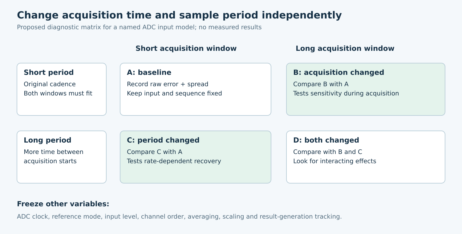
Choose two legal acquisition windows and two legal trigger periods. Both periods must accommodate the configured conversion sequence. Keep ADC clock, reference, input voltage, channel order, and processing unchanged. The four configurations are a proposed experiment, not reported measurements:
- Short window, short period: establish the original operating point.
- Long window, short period: change acquisition time while keeping overall sampling cadence fixed, if the hardware schedule permits it.
- Short window, long period: provide more time between samples without extending the acquisition itself.
- Long window, long period: check whether the two changes interact.
If only the longer acquisition window helps, investigate charging and settling during acquisition. If extra time between samples helps while the acquisition window is unchanged, investigate external-node recovery, reference behavior, or another rate-dependent interaction. If both help, preserve both hypotheses until a circuit model and waveform support a narrower conclusion.
If neither helps, return to input range, reference error, gain/offset configuration, data alignment, and result freshness. The matrix is a way to direct investigation, not a proof that every rate-dependent error is caused by source impedance.
4. Challenge channel history deliberately
TI’s input-circuit evaluation report explains that settling behavior depends on converter architecture and the sampling capacitor’s starting condition. A design that repeatedly measures one steady input may behave differently when it alternates among channels at different levels.
Add controlled sequence tests: repeat one channel, alternate two well-separated safe levels, and reverse their order. Compare the first reading after a channel change with later readings. Keep the voltage source within all normal input limits; a near-rail test must not exceed those limits through tolerance or transients.
If the error follows the previously selected channel, document that dependency before adding a discarded sample as a workaround. A discard may consume time and change charge history without establishing adequate settling across the complete operating range. Any workaround needs its own throughput and worst-case sequence qualification.
5. Select a remedy with an explicit tradeoff
A longer acquisition window may be the simplest remedy when the application’s latency and throughput budget permits it. Confirm the actual programmed duration and the manufacturer’s minimum requirements. Do not assume that reducing ADC clock or interrupt frequency creates the same change.
A lower-impedance source or suitable buffer may support a shorter window, but it changes the analog design. Verify input/output range, supply conditions, noise, transient response, and stability. TI’s capacitive-load discussion shows why an amplifier driving capacitance can ring or settle slowly. Adding capacitance at the ADC pin is therefore not an unconditional improvement.
Evaluate a proposed RC network together with the source and ADC model. A reservoir capacitor can influence the immediate charge demand and the recovery between acquisitions; it also changes bandwidth and loading. The useful question is whether the complete circuit reaches the required error bound in the available time, not whether a capacitor made one static reading look better.
6. Define the release evidence
Prepare a per-channel worksheet containing source circuit, component tolerances, selected reference mode, input-model parameters, acquisition setting, trigger period, sequence, and permitted settling error. Separate the allocated settling error from the ADC’s other error terms rather than spending the whole system accuracy budget twice.
Validate representative low, middle, and high safe input levels, worst intended channel transitions, and the relevant temperature and supply corners. Use a probe whose loading is understood; a large probe capacitance can change the very transient being investigated. Correlate pin observations with raw conversion records and configuration snapshots.
No circuit simulation or ADC measurement was performed for this article. The deliverable is a controlled source/settling/sampling test plan. Completion means the selected input network and acquisition setting meet a stated error budget under the required operating conditions, with evidence that separates analog settling from software timing and stale-data faults.