Low-Power Pin States: Verify Bias and Mux Settings Without Losing the Wake Input
Assign each pin a sleep role before changing its configuration. A wake input must retain a working input path and a defined inactive level, while an unused input may benefit from disconnecting its input buffer. Applying the same low-power setting to both can produce a quiet board that cannot wake.
Applicability: the concrete example uses Nordic nRF52840 Product Specification v1.8, GPIO and System OFF behavior. The board, button, and sensor arrangement is hypothetical. No current reduction, wake latency, or electrical waveform was measured. Other processors require their own pad, retention, and wake-controller contracts.
1. Build a pin-role matrix from the schematic
For every externally connected pin, record the receiving and driving components, both supply domains, active polarity, normal function, sleep function, bias source, and required wake behavior. Include test pads, debug connections, translators, and externally powered connectors. A pin that looks unused in application code can still have an electrical load.
Separate at least four roles: required wake input, unused digital input, output that must hold a safe state, and interface connected to a switched-off peripheral. For each, state who establishes its voltage while the processor is asleep. “Input” or “high impedance” alone does not answer that question.
Use the selected components’ limits to decide whether the state is safe. An output connected to an unpowered receiver needs an off-state injection assessment; changing the processor to input does not remove an external pull-up. Likewise, disabling an internal pull may expose a floating net rather than save useful energy.
2. Preserve the nRF52840 input-buffer dependency
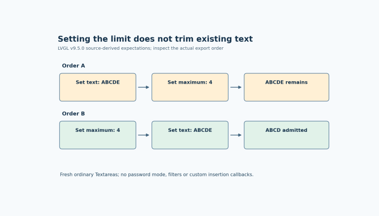
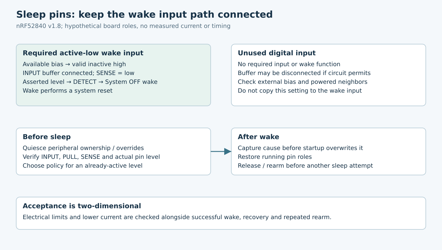
The v1.8 GPIO specification, section 6.9.1, permits disconnecting an input buffer when its pin is not used as an input. It also explicitly requires the buffer to be connected for valid IN-register values and for the SENSE mechanism to access the pin. SENSE configuration alone is therefore insufficient.
In the hypothetical design, an active-low button is biased high from an available supply and pulls the wake input low when pressed. The sleep contract keeps that pin’s input buffer connected, selects low-level sensing, and provides a valid inactive high. The exact bias arrangement and resistance must be justified from the actual board and electrical specifications.
An unused pin with no required digital input or wake function can have its input buffer disconnected where the complete circuit permits it. Do not copy that setting to the button. Review the input-buffer field independently of direction, pull, and sensing fields; a register dump that shows only SENSE=low misses the decisive dependency.
3. Distinguish retained configuration from retained ownership
The same specification identifies PIN_CNF as retained registers and describes GPIO sensing as functional in System ON and System OFF. Those facts support a sleep-state design, but do not prove that a particular firmware path installed the intended configuration before entering that mode.
Read back the relevant configuration immediately before the transition when possible. Record peripheral ownership as well: Nordic documents that other peripherals can override GPIO output and configuration. A GPIO register value may not describe the effective pad behavior while a peripheral still controls it.
Quiesce the owning peripheral using its documented sequence before changing an interface pin’s sleep role. Avoid reusing a pin as a wake input while another block can drive or override it. Keep the selected mux/function and the GPIO configuration together in the review record, even on devices where these controls are not exposed through one software abstraction.
4. Handle a wake level that is already active
GPIO SENSE is level detection. The specification says an already-matching level asserts DETECT immediately when sensing is enabled. Treat a button held during sleep entry as a defined branch, not as a missing future edge.
Choose an explicit product policy. It may defer entry until the input becomes inactive, accept immediate wake, or process the pending request before trying again. Do not clear a software event and assume the physical level disappeared. Record both the sampled input and the intended sensing level at the transition.
The manufacturer’s GPIO chapter also distinguishes the shared DETECT signal from individual pin sensing. If several pins are enabled, log their configurations and available cause information rather than assuming the last configured pin caused the wake. Use the selected DETECTMODE and latch behavior consistently; this article does not prescribe a universal latch-clearing sequence.
5. Treat System OFF wake as a restart path
The v1.8 POWER chapter states that a wake from System OFF performs a system reset. The application must therefore review startup as well as the code immediately after its sleep request. A retained GPIO configuration can be overwritten by board initialization before application-level logging begins.
Capture relevant reset and wake evidence early, following the register’s documented clearing rules, then restore the intended running pin roles. Preserve enough information to distinguish an immediate held-level wake from an unrelated restart. Do not promise that a later high-level button handler will observe the original electrical condition.
Before the next sleep attempt, confirm the input has reached the policy’s rearm condition. A continuously held button can otherwise produce repeated entry-and-wake behavior. Make that behavior bounded and observable rather than hiding it behind a generic low-power retry loop.
6. Exercise the electrical and functional branches
Propose a controlled fixture with the actual supply arrangement and safe externally driven input levels. Test an inactive input through entry, an assertion after entry, a held-active input before entry, release after wake, and a second sleep/wake cycle. Include every permitted peripheral-supply state.
Observe the wake pin at the device, relevant supply rails, and a boot or application marker. Use a stimulus duration justified for the real device and product; no minimum pulse width is inferred here. Confirm useful application recovery, not merely a change in measured current.
Then compare current with one approved pin-state change at a time. Nordic warns that digital input voltages between VIL and VIH can increase consumption, so inspect ambiguous levels instead of assuming all excess current is firmware activity. Instrument connections can themselves bias the node; document them.
7. Release a state contract, not a blanket rule
The resulting artifact should contain the schematic-level pin matrix, pre-entry register snapshot, ownership transition, wake/rearm policy, and fixture observations. Mark unmeasured states and unknown off-state limits as unresolved.
Accept a change only when it preserves the required wake cases and satisfies the electrical limits across the supported supply sequence. A lower sleep-current reading is useful evidence, but it cannot compensate for a disconnected wake input or an undefined receiver voltage.