Charge-Output Vibration Sensors: Decide Whether Cable Capacitance Belongs in the Gain
A replacement cable can change the measured amplitude of a charge-output piezoelectric sensor even when the sensor and physical vibration are unchanged. Whether that happens depends on the input architecture. A high-impedance voltage input and a charge amplifier do not interpret the same sensor in the same way.
For a gateway interface, the first question is therefore what the sensor actually delivers and what the front end measures. A charge-output piezoelectric element should not be treated as an IEPE voltage-output sensor simply because both may appear in vibration monitoring. Their excitation and conditioning requirements are different.
Start with the sensor’s electrical model
Over a suitable operating band, a simplified piezoelectric sensor model represents the generated charge together with the sensor capacitance. A voltage-reading input also sees cable and input capacitance. Neglecting leakage and other dynamics for this initial model, the voltage associated with a charge change Q is Q divided by the total capacitance.
That denominator matters. The cable is not merely a route for an already established low-impedance voltage. Adding capacitance changes the conversion between generated charge and observed voltage. The valid frequency range and additional sensor behavior still come from the selected device and complete circuit.
Analog Devices’ discussion of high-impedance sensors contrasts a noninverting voltage-amplifier approach with a classical inverting charge amplifier. The former can be attractive when parasitic capacitance remains small and stable; the latter avoids putting cable capacitance directly into the ideal charge-to-voltage gain.
A hypothetical cable change shows the distinction
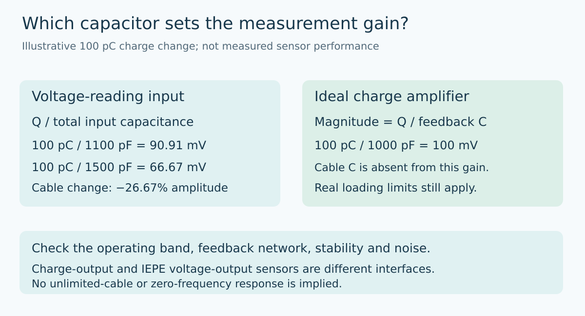
Suppose a sensor generates a charge change of 100 pC and has 1000 pF capacitance. Assume the first cable and amplifier input contribute another 100 pF. An ideal voltage-reading input sees 100 pC divided by 1100 pF, approximately 90.91 mV.
Now replace that cable with an assembly that brings the combined cable and input contribution to 500 pF. The same charge change produces 100 pC divided by 1500 pF, approximately 66.67 mV. The second amplitude is about 26.67% lower than the first.
These are illustrative values, not sensor or cable specifications. No vibration measurement was performed. The example isolates capacitance sensitivity; it does not include leakage, amplifier bandwidth, mechanical cable noise, or the sensor’s complete transfer behavior.
Calibrating the first assembly as a whole can hide this dependence until the cable changes. A replacement with the same connector and adequate continuity may still fall outside the original amplitude calibration. The relevant installation requirement may therefore include capacitance, not only cable length or conductor resistance.
A charge amplifier changes the controlling capacitor
In the ideal charge-amplifier operating region, feedback holds the input node near the reference potential and the generated charge is balanced by charge on the feedback capacitor. The output change has magnitude Q/Cf, where Cf is the feedback capacitance. Polarity follows the actual connection and inverting topology.
For the same 100 pC example and a hypothetical 1000 pF feedback capacitor, the output-change magnitude is 100 mV. Cable capacitance does not appear in that ideal gain expression. Analog Devices’ CN-0350 uses this charge-to-voltage relationship in a practical piezoelectric acquisition circuit.
This does not mean that any cable can be attached without consequences. The amplifier must maintain the required feedback behavior over the intended frequency range and input capacitance. Real stability, noise, leakage, protection, and output range still constrain the design. “Cable-independent gain” is a model property, not an unlimited cable specification.
Keep the feedback resistor in the model
A practical charge amplifier generally includes a DC feedback path, commonly a resistor in parallel with the feedback capacitor. That path prevents the circuit from behaving as an ideal integrator indefinitely. Together with the capacitor, it also sets a low-frequency boundary for the charge response.
For a simple ideal feedback network, the characteristic frequency is 1/(2πRfCf). With hypothetical values of 100 MΩ and 1000 pF, it is approximately 1.59 Hz. The Q/Cf gain should not be presented as a flat response down to zero frequency. Use the complete transfer function when the wanted vibration approaches that boundary.
Feedback capacitance tolerance and parasitics also affect the scale. If a nominal capacitor is small enough that layout capacitance is material, the effective value can differ from the component label. The desired gain needs to be connected to the assembled feedback network, not just the nominal bill-of-materials value.
Preserve input identity in the connector contract
The interface drawing should state that the supported sensor is charge-output, identify its reference and polarity, and describe the permitted cable arrangement. Do not enable an IEPE constant-current source on that input unless the sensor and architecture explicitly require it. A connector shape does not identify an electrical interface.
Where a product supports multiple front-end modes, keep the mode tied to the installed sensor definition and supported switching sequence. A software menu that changes scaling alone cannot transform a voltage input into a charge amplifier. The physical input configuration and reported units must agree.
Likewise, distinguish charge sensitivity from voltage sensitivity in configuration data. Converting a sensor’s pC-per-unit specification using a remembered voltage gain from another input mode creates a plausible but unjustified number. Store the relevant sensitivity, front-end scale, and calibration scope together.
Make cable replacement a defined event
For a voltage-mode architecture, document the capacitance conditions included in calibration and decide which replacements require a new calibration or characterization. For a charge amplifier, document the supported capacitive load and the evidence for acceptable response and noise over that range.
A useful electrical comparison holds a known charge stimulus and feedback network constant while changing only a representative input capacitance within the circuit’s limits. Interpret the result with the stimulus fixture’s own capacitance and leakage included. This is a proposed model check, not an executed acceptance test.
The final design decision is not that one topology is universally better. It is whether cable variation belongs in the measurement gain or is primarily an input-loading constraint. Naming that distinction early prevents a maintenance cable replacement from silently becoming an amplitude recalibration.
Primary references and trend scope
Analog Devices, Signal Conditioning for High Impedance Sensors, section 7 compares the voltage and charge approaches. Analog Devices CN-0350, Revision A, Circuit Design provides the charge-conversion foundation. Numerical examples are original hypothetical calculations.
The preserved Google Trends RISING row “industrial iot solutions,+110%,” worldwide, all categories, web search, July 19–October 19, 2026 supports the parent integration topic, not claimed growth for charge-output sensors or this title.