Gateway LDOs: Check Reverse Current When the Input Rail Collapses
An LDO can regulate a gateway’s analog rail correctly during normal operation and still create an unwanted current path during shutdown. If its input falls faster than its output, stored energy or another powered interface can make the output higher than the input. The relevant question is no longer dropout voltage. It is where current can flow when the normal voltage ordering reverses.
This review concerns low-voltage board rails. It uses Texas Instruments’ LDO Basics: Preventing Reverse Current, SSZT658, July 2018, pages 1–4, and the TPS7A37 datasheet, SBVS220B, revised August 2015, pages 5 and 12–13. All calculations are illustrative models, not device stress limits or measured waveforms.
Draw the shutdown circuit, not just the running circuit
During operation, an upstream converter may hold the LDO input at 5 V while the output supplies 3.3 V. During shutdown, the upstream converter might actively discharge its rail, remain high impedance, or be pulled down by another load. Those cases produce different reverse-current consequences.
List the output capacitance and every possible source still connected to the output domain. Include sensor supplies, debug connections, and digital interface paths where the actual component documentation permits or describes injection. A schematic power symbol does not prove that a rail becomes unpowered when its primary source is disabled.
Also identify the intended receiving node for any discharged energy. Feeding an unpowered upstream rail can partially energize circuitry that the system assumes is off. Clamping that node hard to ground can instead create a substantial transient current. Neither outcome is adequately described by “the LDO is disabled.”
Estimate how long the output can remain elevated
Consider a hypothetical 220 µF output capacitor initially at 3.3 V and a constant 10 mA downstream load. With no reverse path, its voltage falls at I/C, approximately 45.45 V per second. Losing only 0.3 V takes 6.6 ms.
If the input were to collapse from 5 V to zero within 1 ms, the output-only model would still predict approximately 3.255 V at that instant. This demonstrates a plausible voltage inversion. It does not predict the actual output once a reverse path begins conducting, because that path changes the current balance.
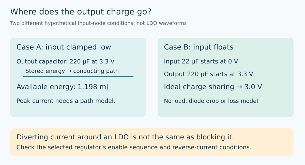
The capacitor initially stores approximately 1.198 mJ. That energy calculation identifies the quantity available for redistribution, but not its peak current. Peak current depends on the conducting path’s dynamic impedance, interconnect inductance, and source behavior. Dividing stored energy by an arbitrary time is not a substitute for the selected regulator’s reverse-current specification.
Distinguish diversion from blocking
TI’s reverse-current article describes several topology options. One is an external diode from output to input, oriented to conduct when output exceeds input. It can divert current away from a vulnerable internal path. It does not, by itself, prevent energy from reaching the upstream input node.
That distinction matters in a gateway with independently controlled domains. A protection arrangement suitable for preserving a regulator during a transient may be unsuitable if the system also requires isolation between rails. Name both requirements: protect the regulator and prevent unintended upstream energization.
An input-series blocking element addresses a different boundary and introduces its own forward loss and voltage headroom. Back-to-back switching structures can provide another approach, but their control conditions and ratings remain device-specific. Do not convert a topology sketch into an unrestricted promise of zero reverse current.
Check the input node’s destination
A second hypothetical model illustrates why upstream behavior matters. Suppose the input is disconnected and initially discharged, with 22 µF remaining on that floating node. If it is then connected ideally to the 220 µF, 3.3 V output capacitor, charge conservation predicts a final common voltage of 3.0 V, before other loads and diode effects.
That is not a model of an input clamped to ground, and it is not an actual LDO waveform. It simply demonstrates that a small floating input capacitor can rise substantially when charge is redistributed. In the clamped-input case, the same output energy is dissipated through a different network instead.
Therefore, record whether the upstream device can sink current, how its shutdown mode behaves, and which circuits share that rail. A bench supply that absorbs reverse current can mask a field source that cannot. Conversely, a bench supply’s protective response can add a behavior that is absent from the intended system.
Read the conditions behind reverse-current protection
TPS7A37 is a useful example of why the feature name is insufficient. Its section 7.3.3 requires EN to be driven low before removing input voltage so that the pass device’s gate charge is removed. Otherwise, the pass element may remain on. After the documented disable sequence, the protection does not require an applied bias voltage.
The datasheet also distinguishes current exiting the input pin from current drawn by the output-side internal divider, and notes an additional feedback-pin condition for the adjustable version. Those boundaries prevent an incorrect interpretation of “reverse leakage” as the entire output discharge current under every state.
For the chosen regulator, build a state table covering enabled, disabled, input absent, output externally driven, and all supported sequencing orders. Use guaranteed limits where available. Typical curves and a favorable topology description do not create a maximum rating that the vendor has not specified.
Observe the crossing and its consequences
Plan a current-limited low-voltage test that captures input voltage, output voltage, enable, and current in the relevant return path. Define polarity before interpreting the current trace. Ensure probe connections do not introduce a second ground path or exceed instrument ratings.
Compare the intended controlled shutdown with abrupt source removal only when both are supported product conditions. Include the smallest and largest effective output capacitances and the still-powered interface configurations the product actually allows. Do not create uncontrolled shorts to simulate a fast collapse.
The acceptance record should show that the regulator remains within its documented limits, the upstream rail does not enter an unintended powered state, and the output reaches its required shutdown condition. Forward regulation and reverse isolation are separate specifications. Reviewing both before layout is far cheaper than discovering their difference through an intermittent power-cycle failure.
Topic provenance
The preserved Google Trends RISING row “industrial iot solutions,+110%,” worldwide, all categories, web search, July 19–October 19, 2026 supports the parent integration topic only. It does not establish search growth for this electrical mechanism or article title.