STM32G474 to STM32G431: Decide Whether the Cost-Down Fits Before Porting
The STM32G431 can be a sensible smaller replacement for an STM32G474 design, but matching the Cortex-M4 core and maximum clock is not a migration argument. The decision turns on resources that disappear, resources that shrink and functions that the board cannot reproduce through software alone.
Use the exact ordering codes on both sides. This comparison uses ST's G431 datasheet, DS12589 Rev 6, G474 datasheet, DS12288 Rev 6, and the product-specific feature table in RM0440 Rev 9. It establishes an architectural screening method, not price savings, drop-in compatibility or a tested firmware port.
Start with dependencies that cannot be optimized away
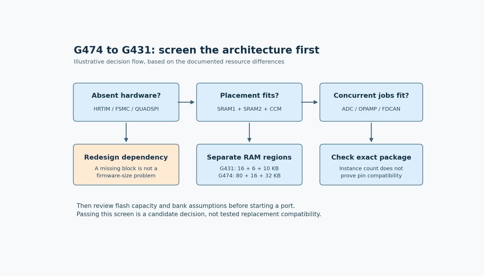
RM0440 lists HRTIM on G474 and excludes it from G431. A design that depends on that timer's particular resolution, event routing or protection behavior needs a timer redesign before it can move. The presence of advanced-control timers on G431 does not establish equivalent timing behavior.
The same table excludes both FSMC and QUADSPI from G431. If the current board uses either interface, the proposal includes an external-memory architecture change. Calling a serial device through another SPI controller may be possible in a redesigned product, but it is not preservation of a memory-mapped Quad-SPI interface.
Make a dependency record from the running design: peripheral instance, pins, trigger relationships, DMA request, timing requirement and fallback. An empty fallback is a useful early rejection, especially when the smaller device was chosen before anyone reviewed the schematic.
Treat the RAM map as several budgets
G431 has 32 KB of SRAM in total: 16 KB SRAM1, 6 KB SRAM2 and 10 KB CCM SRAM. G474 provides 128 KB, divided into 80 KB SRAM1, 16 KB SRAM2 and 32 KB CCM SRAM. Those totals are not interchangeable linker regions.
Compare the existing linker map with the proposed target map. Separate initialized data, zero-initialized data, stacks, heap limits, DMA buffers and any explicitly placed time-critical routines. A total below 32 KB is only the beginning; each placement must fit a valid region and satisfy the access requirements of its users.
For example, an illustrative design using 24 KB of ordinary SRAM plus 12 KB explicitly allocated to CCM fails two independent G431 limits. Reducing the total to 31 KB would not resolve a 12 KB CCM allocation. These figures describe a hypothetical placement problem, not a measured project.
Preserve peak-runtime evidence as a separate requirement. A static map cannot establish the maximum stack depth of interrupt nesting or a variable-sized communication workload. The port should not rely on an unexplained reduction in reserve simply to make the linker succeed.
Flash capacity and bank topology both change
G431 ordering options reach 128 KB of flash, while G474 options reach 512 KB. RM0440 also identifies G431 flash as single bank and G474 flash as dual bank. An existing updater's assumptions therefore deserve review even when its two linked images happen to fit the proposed address space.
Inventory boot code, application, immutable data, calibration storage and update staging. Then identify which operations require code or interrupts to run while flash is being modified. Do not infer an unchanged update strategy from identical application APIs; bank topology is a hardware property beneath that API.
This screening step does not prescribe an updater. Its output is the precise feature that must be redesigned or separately qualified, rather than a vague instruction to optimize firmware size.
Count independent analog and communication jobs
The G431 has two ADC instances, three OPAMPs and one FDCAN instance. The G474 has five ADCs, six OPAMPs and three FDCANs. Both contain CORDIC and FMAC, so a smaller part does not automatically mean losing those accelerators.
Count simultaneous jobs, not only channel names. Three signals sampled at different times might fit a two-ADC architecture; three independently constrained conversion schedules need a timing argument. Likewise, two independent CAN buses do not become one because their software stacks share source code.
After the instance count fits, inspect the exact package's pin table and internal routing. A peripheral present on the die does not guarantee a compatible pin assignment. The comparison table cannot establish that an existing PCB footprint is reusable.
Finish with a decision that exposes the redesign
A useful result has three outcomes. A hard dependency on missing hardware rejects a direct substitution. A resource deficit with an identified architectural change becomes a redesign proposal. A design that fits the documented resources becomes a candidate for an actual port and qualification campaign.
Attach the two ordering codes, the memory-region worksheet, missing-resource list and required timing changes to that decision. Record commercial savings separately using a real quotation; no price or availability comparison was performed here.
The value of this early review is avoiding a misleading milestone. A successful compile on a G431 target proves much less than a supported replacement for a G474 board. The replacement becomes credible when its real workload has somewhere to live and every hardware dependency has an explicit implementation.