TXB0108 Gateway Expansion Ports: Check the One-Shot Load Before Blaming Firmware
A translated GPIO works on the bare gateway board but becomes unreliable when an expansion cable or accessory is attached. Firmware timing is an obvious suspect, yet the interface may have crossed an electrical limit of its auto-direction translator. A TXB0108 is not simply a pair of strong buffers that happen to choose direction automatically. Its edge assistance and steady-state drive have different jobs.
The source for this example is Texas Instruments’ TXB0108 datasheet, SCES643L, revised February 2026. Sections 7.3.1–7.3.5 on pages 16–17 describe direction sensing, one-shot acceleration, output loading, enable timing, and external pull resistors. The following calculations explain the architecture; they are not device characterization or a universal recommendation to use this part on an expansion connector.
Separate the edge accelerator from the static output
The TXB0108 architecture lets an external driver override the translator’s weak steady-state drive when direction changes. One-shot circuits briefly provide stronger assistance during transitions. That arrangement is useful only when the connected circuit fits the intended behavior.
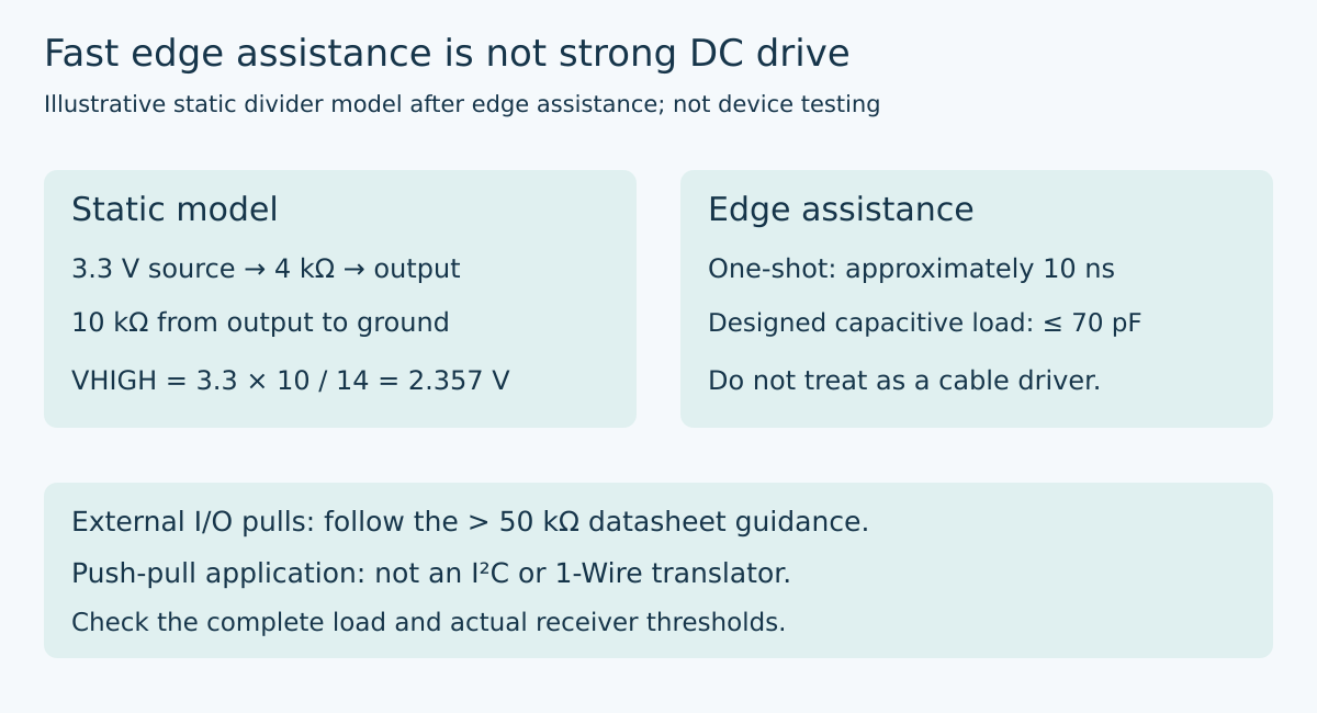
Section 7.3.3 describes an approximately 10 ns one-shot duration. It also warns that a very heavy capacitive load can leave the output short of its positive rail when that assistance ends. A subsequent slow movement toward the rail is therefore not necessarily a software pulse that was deliberately shaped that way. It may reflect the change from transient assistance to weaker drive.
Do not treat the approximate one-shot duration as a guaranteed minimum pulse width or derive a supported interface rate from its reciprocal. Timing guarantees belong to the applicable switching-characteristics tables and test conditions. The architecture explains a failure mechanism, not a substitute operating specification.
Count the load that the accessory adds
Section 7.3.5 states that the device is designed to drive capacitive loads up to 70 pF. That figure does not make every 70 pF connection equivalent. The preceding section also discusses trace length and reflection timing: a distributed cable and a compact lumped capacitor can interact differently with the one-shot circuit.
For a hypothetical compact load estimate, suppose the receiver contributes 8 pF, local routing and connector contribute 12 pF, and a proposed accessory adds 35 pF. The total is 55 pF before tolerance, test fixtures, or probe loading. Adding a 15 pF probe raises the nominal total to 70 pF. These values are illustrative estimates, not specifications for actual components or a claim that the unprobed circuit qualifies.
This example explains why a measurement connection can change the symptom. It also shows why counting only the receiving IC’s input capacitance is inadequate. Record the entire permitted accessory population and its physical interconnect, then determine whether a lumped model is appropriate. A long lead does not become a short board trace merely because its capacitance appears below a headline limit.
External pull resistors can oppose the static driver
The datasheet’s section 7.3.5 directs external I/O pullups or pulldowns to remain above 50 kΩ because of the low DC drive strength. A default 10 kΩ resistor copied from a generic GPIO circuit can therefore be a material load in this architecture.
Use a simplified model to see the consequence. Suppose a high output is represented by an ideal 3.3 V source through 4 kΩ, consistent with the approximate internal resistance shown in the architectural diagram. A 10 kΩ external pulldown forms a divider. The calculated output is 3.3 × 10/(4 + 10), or approximately 2.357 V.
With a 100 kΩ pulldown, the same idealized calculation gives 3.3 × 100/(4 + 100), approximately 3.173 V. This is not a guaranteed VOH for either resistor: real output behavior, internal variation, rails, leakage, and receiver requirements remain. The comparison simply demonstrates why a strong-looking transition does not ensure an adequately held logic level after edge assistance ends.
Check receiver thresholds at the actual receiver supply and operating conditions. Do not assume that a nominal “3.3 V signal” has sufficient high-level margin merely because the rising edge briefly approached 3.3 V. Capture the level during the required sampling interval, not only the peak.
Confirm that the interface is push-pull
The TXB0108 datasheet explicitly excludes applications such as I2C and 1-Wire with an open-drain driver on the bidirectional data I/O. Those interfaces depend on behavior that is different from a push-pull signal overriding a weak opposing output. Replacing pullups or slowing the transaction does not change that architectural mismatch.
For an expansion connector, document whether each signal is push-pull, open-drain, tri-stated during turnaround, or driven by multiple devices. Do not infer the electrical mode from a signal name. A peripheral interrupt may be open-drain even when neighboring SPI signals are push-pull, so one translator choice need not fit every pin in the connector.
When the connected device can actively drive in the opposite direction, establish the ownership sequence as well as the electrical compatibility. Auto-direction sensing is not arbitration permission for two strong drivers to contend. A direction-controlled translator or another architecture may be more appropriate when the system needs explicit direction, stronger drive, or different load support.
Diagnose one load boundary at a time
Begin with the approved board configuration and a repeatable push-pull stimulus. Compare captures with the accessory disconnected and connected, preserving voltage rails and acquisition settings. Record the resistor population and probe loading. Look separately at the initial transition, the level after the one-shot interval, and behavior during any direction change.
If reducing repetition rate appears to help, verify whether the receiving device simply gets more time to sample a slow edge. That observation does not establish acceptable noise margin or remove reflection-induced retriggering. Likewise, removing a pull resistor may improve a driven level while leaving the required idle state undefined. Each modification needs a complete interface argument.
The release outcome should be a bounded port specification: supported drive modes, rail relationship, accessory load and interconnect, pull-resistor constraints, and receiver-side timing/level evidence. Without those boundaries, an expansion connector can silently turn a qualified local GPIO path into an unsupported transmission system.
Primary reference and trend scope
Texas Instruments TXB0108 datasheet, SCES643L, February 2026 revision, sections 7.3.1–7.3.5, pages 16–17. Divider and capacitance values are hypothetical calculations; no hardware performance is claimed.
The preserved Google Trends RISING row “industrial iot solutions,+110%,” worldwide, all categories, web search, July 19–October 19, 2026 supports the gateway parent topic only. It does not show rising demand for TXB0108 or this article title.