STM32H563 EDATA: Qualify Capacity, Endurance and Serviceability Together
STM32H563 high-cycle flash can be useful for configuration data, but enabling EDATA is a memory-layout and silicon-qualification decision. It consumes code-flash sectors, changes their usable data capacity and can interact with the service lifecycle on affected revisions. A “100 kcycles” headline alone does not establish that external storage can be removed.
This article scopes the H562/H563/H573 organization in RM0481 Rev 5, DS14258 Rev 6 and ES0565 Rev 8. It addresses the physical storage choice; it does not implement a power-fail-safe EEPROM-emulation algorithm or claim endurance measurements.
Count the code capacity you give up
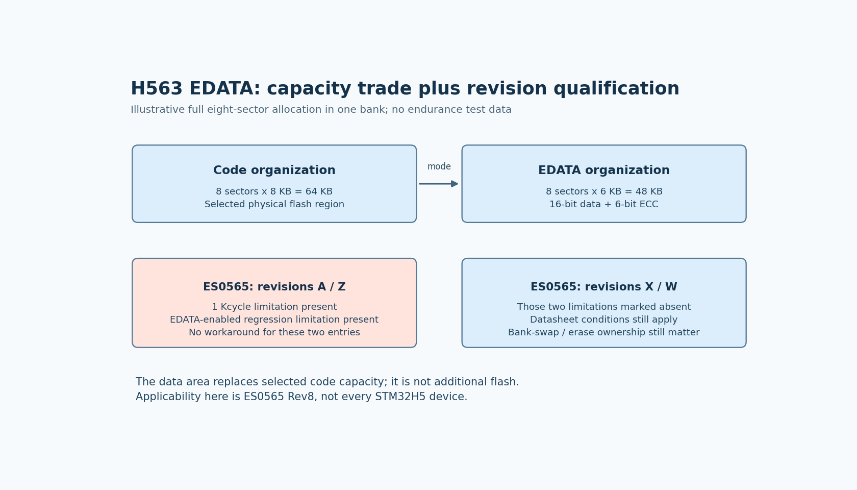
RM0481 section 7.3.10 describes a high-cycle data area formed from selected final sectors of each flash bank. Normal sectors have 8 KB capacity; the selected data sectors provide 6 KB with 16-bit data granularity and 6-bit ECC. The documented maximum is 48 KB per bank, or 96 KB across both banks.
For the illustrated full eight-sector allocation in one bank, eight 8 KB code sectors represent 64 KB of code capacity, while the data representation provides eight times 6 KB, or 48 KB. This arithmetic describes the same selected physical region under different organizations. It is not 48 KB of additional storage alongside an unchanged code image.
An application that almost fills the original code bank may therefore fail its layout review even when its configuration records are small. Include the entire reserved EDATA sector set in the linker and image-layout decision, plus any storage-algorithm overhead. Do not budget only the current serialized record size.
Record both the data window and the physical bank
The high-cycle area has its own address window. The manual's Bank 1 example enables 48 KB beginning at 0x09000000. ST's AN4894 EDATA explanation describes the corresponding organization and bank mapping.
SWAP_BANK changes which physical bank appears in each high-cycle window. A boot/update design that swaps banks must account for that association when locating configuration data. An address constant alone does not establish that it still identifies the same physical records after a swap.
Erase operations also refer back to the corresponding user-flash sectors. Keep one mapping from logical record area to data-window address, physical bank and erase-sector identity. The firmware updater and configuration-store implementation must agree on that mapping so an image-maintenance operation does not erase the data area accidentally.
The region is for data: instruction fetch from EDATA produces a bus error. It should not become an overflow destination for executable sections merely because a linker can be made to assign an address there.
Apply the endurance table and the errata together
DS14258 Table 52 distinguishes program-memory endurance from data-memory endurance and gives separate retention conditions. Its data-memory figure is 100 kcycles under the table's stated junction-temperature conditions. Retention after cycling depends on the listed ambient-temperature and cycle-count case. Those parameters cannot be replaced by one unconditional number of service years.
More importantly, ES0565 Rev 8 lists the flash-endurance limitation in section 2.2.13. The applicability table marks revisions A and Z as affected, with no workaround; X and W are marked unaffected. The limitation gives 1 Kcycle at ambient temperatures up to 85°C instead of the stated 100 Kcycle expectation.
Consequently, qualifying a storage design requires an actual silicon-revision policy. Passing repeated writes on one newer sample does not qualify an inventory containing affected older revisions. Conversely, an erratum marked absent on X/W should not be reported as a universal H563 limitation.
Check whether the service plan survives EDATA
Section 2.2.10 adds another A/Z limitation: product-state regression to OPEN is not possible when EDATA1_EN or EDATA2_EN is enabled. The same table marks X/W unaffected, and the entry provides no workaround for affected revisions.
This couples the storage decision to manufacturing and repair. A product whose recovery procedure depends on full regression cannot approve EDATA on an affected revision by demonstrating that normal configuration reads and writes work. The normal runtime path and the required lifecycle transition are separate acceptance obligations.
Use the revision and option configuration as explicit inputs to the storage feasibility decision. If the selected combination cannot meet the required service route, choose a different supported combination or storage architecture rather than leaving recovery as a future firmware task.
Deliver a storage qualification record
The record should state the selected silicon revision, sacrificed code sectors, usable data sectors, bank-swap behavior, erase ownership, expected update workload and applicable endurance/retention conditions. It should also identify the higher-level record-commit and recovery algorithm; EDATA's hardware organization does not by itself create atomic application transactions.
Only then proceed to approved endurance, power-interruption and update-interoperability qualification on disposable units. No such tests were performed here. The architectural result is narrower but valuable: the chosen high-cycle region must fit the image, the operating workload and the product's service lifecycle at the same time.