Gateway Ideal Diodes: Bound Reverse Current Before the MOSFET Turns Off
An ideal-diode controller can block sustained reverse current without making the reverse transient disappear. When a gateway’s input suddenly collapses, its charged output capacitors may briefly feed the failed input through a still-conducting MOSFET. The useful design question is how much current and energy can develop before that path is interrupted.
Analog Devices LTC4359 Revision F is the concrete architectural reference. Its operation section describes temporary reverse conduction during a rapid input drop, followed by fast gate pull-down. The examples here are original low-voltage lumped-circuit calculations, not measured LTC4359 performance or a substitute for the component’s application requirements.
Separate steady blocking from the commutation interval
A fully enhanced MOSFET channel conducts in either direction. The controller must detect the changed voltage relationship and remove gate charge before the channel stops carrying the reverse current. The internal comparator response is only part of the physical event; gate charge, drive conditions, parasitic inductance and the current already flowing also matter.
The LTC4359 electrical-characteristics table specifies a gate turn-off delay with an explicit input-voltage step and a gate-voltage criterion. It is not a guarantee that every board’s reverse current reaches zero within that interval. Do not treat a headline response time as a complete fault-current waveform.
Start the review by drawing the reverse loop. Include the output capacitor, MOSFET, failed-input connection and return path. If redundant supplies feed the same output, include their possible contribution. A current probe on the load branch alone will miss current returning through a different input branch.
Calculate a first-order current envelope
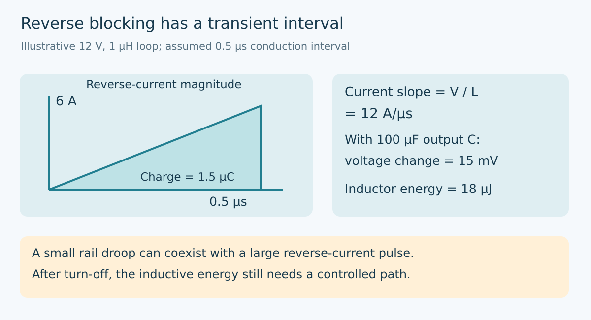
Consider a hypothetical 12 V charged output capacitor connected through an initially conducting switch to an input that has fallen to zero. Assume the reverse loop has 1 µH inductance. Over a short interval in which the capacitor voltage remains approximately constant and resistance is neglected, current slope magnitude is V/L = 12 A/µs.
If the channel continued to conduct for an illustrative 0.5 µs after reverse current began at zero, the calculated current would reach 6 A. The transferred charge is the triangular area, one-half times 6 A times 0.5 µs, or 1.5 µC.
With 100 µF output capacitance, that charge corresponds to only 15 mV of capacitor voltage change. A rail capture with coarse vertical scale could therefore look almost unchanged while a substantial reverse-current pulse occurred. Output-voltage droop and peak reverse current are different observables.
Halving the assumed inductance to 0.5 µH doubles the slope. Under the same intentionally simplified timing assumption, peak current becomes 12 A and transferred charge becomes 3 µC. This comparison is sensitivity analysis, not permission to add uncontrolled inductance. Additional inductance also changes the interruption transient and the required protection network.
A real waveform includes initial forward current, finite resistance, a changing gate voltage and possibly supply current limiting. Those effects require a more complete model. In particular, the chosen 0.5 µs interval is hypothetical and must not be identified as a guaranteed LTC4359 system response.
Account for the energy after turn-off
Current in an inductor cannot vanish instantaneously. At 6 A and 1 µH, the stored magnetic energy is one-half LI², or 18 µJ. The circuit must redirect or absorb that energy as the conducting path is interrupted. That is why checking only the MOSFET’s forward conduction loss leaves a gap.
As a separate illustration, transferring 18 µJ into an ideal 100 nF capacitor initially at 12 V would raise it to √(12² + 2E/C), approximately 22.45 V. This is not the predicted voltage on any particular gateway node: actual clamps, distributed capacitance and current paths determine that. The calculation simply shows how modest energy can produce a large voltage change when the receiving capacitance is small.
Use the actual protected node and its initial voltage when applying an energy calculation. A large bulk capacitor elsewhere on the schematic does not automatically absorb a fast local transient through an inductive connection. Component placement and the return path belong in the protection review.
The LTC4359 application information specifically discusses reverse-recovery spikes and protection during input short-circuit faults. Follow that circuit-level guidance, including the applicable MOSFET gate and drain voltage constraints, rather than assuming the controller’s operating-voltage range covers every transient at every pin.
Shutdown is a separate topology question
Turning off one ideal-diode MOSFET does not necessarily disconnect forward power, because its body diode remains. LTC4359 documentation distinguishes a single-MOSFET ideal diode from the back-to-back arrangement used when forward load switching is also required.
For a gateway service mode, write the desired behavior explicitly: prevent the output from feeding a failed input, disconnect the input from the load, or both. Those are different requirements. An enable signal cannot change the orientation of a body diode already present in the power path.
This topology check should precede firmware work. A shutdown command that correctly lowers the gate can still leave the output energized through the intended body-diode direction. That result is not evidence that the digital control failed.
Verify with controlled, bounded conditions
Use a qualified low-voltage fault fixture with current limiting and appropriate transient ratings. Do not reproduce an input short by casually bridging a live supply connector. Begin with a model and the manufacturer’s protection recommendations, then define the allowed voltage, capacitance, initial load and fault impedance for the test.
Capture input voltage, output voltage, gate-to-source voltage and reverse-path current together when the equipment permits. Record bandwidth and probe loading. Compare observed stress with the controller and MOSFET limits, including the protected transient nodes, not only with whether the gateway rebooted.
The release record should identify both the steady-state reverse-blocking behavior and the transient envelope. An ideal diode reduces forward loss; it does not remove the need to account for detection, charge removal and the energy already circulating when a source fails.
Primary reference
The preserved Google Trends RISING row “industrial iot solutions,+110%,” worldwide, all categories, web search, July 19–October 19, 2026 supports the parent integration topic only. It does not establish search growth for this electrical mechanism or article title.