Gateway Hot-Swap MOSFETs: Check the Startup Trajectory Against SOA
A low-resistance MOSFET can be an excellent steady-state power switch and a poor choice for charging a gateway’s bulk capacitor. During controlled startup it may carry substantial current while supporting most of the supply voltage. The resulting stress belongs to its linear-mode safe operating area, not merely its advertised current rating or fully enhanced resistance.
Texas Instruments TPS2490/TPS2491 datasheet SLVS503F, revised February 2020, supplies the architectural reference: separate power and current limiting, with design checks for startup, a short applied during operation, and startup into a short. The calculations here describe an original hypothetical 24 V DC circuit. No MOSFET has been selected or qualified by this example.
Draw the charging trajectory
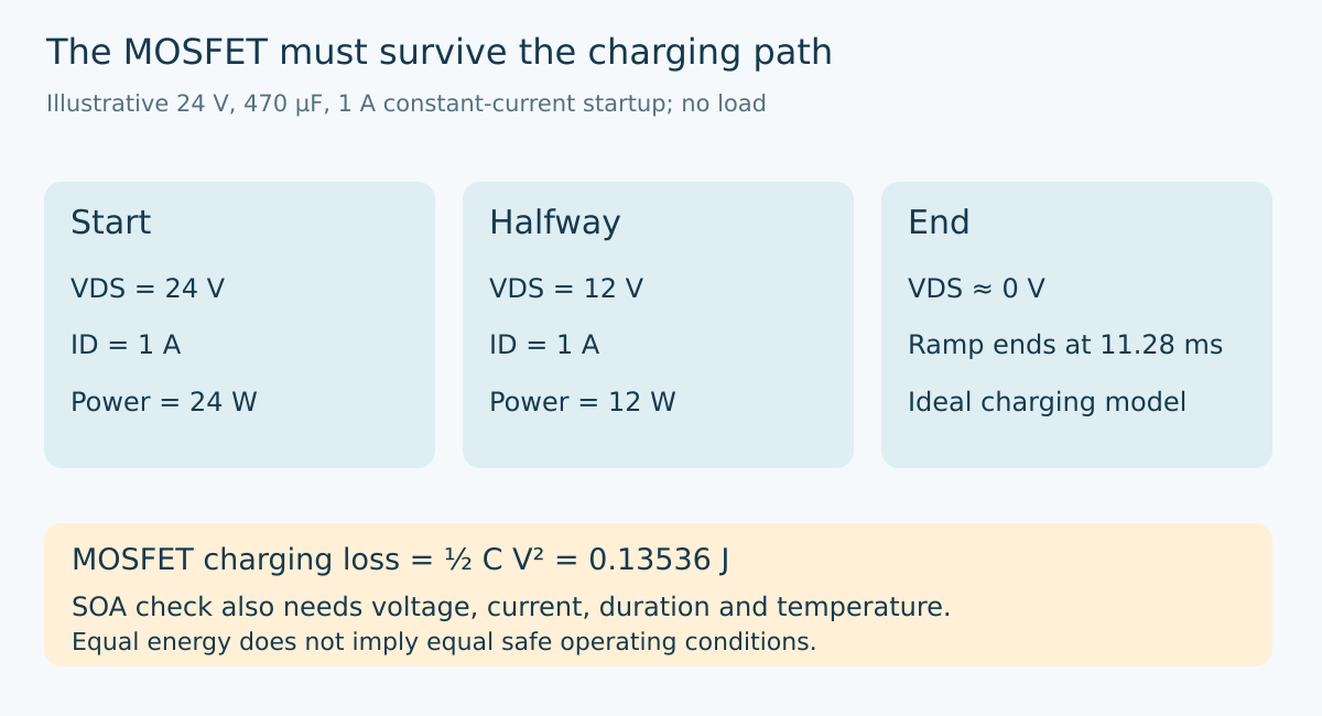
Assume an ideal 24 V source, an initially discharged 470 µF capacitor, and a pass MOSFET that maintains exactly 1 A of capacitor-charging current. Hold the downstream load off. Ignore wiring losses and capacitor ESR for this first calculation.
Capacitor voltage rises at I/C, approximately 2.128 V/ms. Reaching 24 V takes CV/I = 11.28 ms. During that interval, the MOSFET’s drain-to-source voltage falls approximately linearly from 24 V to zero while its current stays at 1 A.
Its initial dissipation is therefore 24 W, falling to 12 W halfway through the ramp and approaching zero at the end of the ideal charging interval. This is nothing like the fully enhanced I²R operating point. For comparison, a hypothetical 10 mΩ fully enhanced resistance would dissipate only 10 mW at 1 A. The same current produces radically different stress because the voltage across the transistor is different.
The useful drawing is a voltage-current-time trajectory. Label the initial point, duration and temperature assumptions. A single average-current number discards the information needed to evaluate the pass element.
Calculate energy without treating it as the only limit
Integrating the linearly falling dissipation gives one-half CV², approximately 0.13536 J in this model. The capacitor stores another 0.13536 J. The ideal source supplies 0.27072 J during charging, so half reaches the capacitor and half is dissipated in the pass path under the stated assumptions.
Reducing the charging current to 0.5 A doubles the ramp time to 22.56 ms and halves initial dissipation to 12 W. The total charging loss remains 0.13536 J. Slowing the ramp changes how the stress is distributed in time; it does not remove the energy that the pass element must handle in this simple circuit.
Equal energy is not an interchangeable SOA condition. The permissible current at a particular drain voltage can depend strongly on pulse duration and initial device temperature. Localized die heating can impose a limit that a package-average energy estimate misses. Conversely, a lower-power, longer pulse is not automatically safer for every transistor and mounting condition.
Use the MOSFET manufacturer’s actual SOA information and its stated test conditions. Do not infer linear-mode capability from an avalanche-energy rating, a large pulsed-current headline or a low resistance measured with the gate fully enhanced.
Use a conservative bound, then justify refinements
For the example, a rectangle at 24 V and 1 A lasting 11.28 ms bounds the ideal declining-power trajectory from above. Checking that rectangle against applicable derated SOA is a conservative first screen. It is not a claim that the transistor actually dissipates 24 W throughout the ramp.
If the rectangular screen is too restrictive, a more detailed thermal and SOA evaluation may use the actual time-varying waveform, provided the device manufacturer supports the method. Do not simply select a shorter pulse curve because the power falls halfway through startup. The earlier part of the pulse has already heated the device.
Likewise, a case temperature printed beside a datasheet curve is a boundary condition, not a prediction for an enclosed gateway. Determine the relevant initial case or mounting temperature and the permitted derating method. Repeated starts also need the prior thermal state; a single-pulse graph does not establish arbitrary repetition capability.
Add the load only after defining what is controlled
If the controller fixes total pass current at 1 A and a hypothetical load already draws 0.2 A, only 0.8 A remains for charging. The ideal charging time becomes 14.10 ms. The MOSFET continues to carry the full 1 A, so the longer event changes its energy and thermal stress.
Under those deliberately constant-current assumptions, its loss becomes one-half times 24 V times 1 A times 14.10 ms, or 0.1692 J. The change is not accounted for by increasing capacitor size in the original equation. It comes from a load consuming current while the pass element still supports a large voltage.
Real downstream converters may draw little current below a startup threshold and then demand considerably more. Their input behavior is not necessarily a constant 0.2 A. Holding them disabled until the input capacitor has charged can simplify startup, but that sequencing must follow the actual enable and supply requirements. A firmware delay cannot control circuitry that starts before the processor runs.
Keep fault scenarios separate
During a sustained output short, the capacitor does not complete a normal ramp toward the source voltage. The pass element may continue supporting nearly the full input until protection terminates the event. Therefore, a startup calculation cannot establish short-circuit survival.
The TPS249x design procedure addresses the fault timer and MOSFET power limit together with SOA. Follow the selected controller’s limits, tolerances and retry behavior. A power limit constrains instantaneous dissipation but does not, by itself, establish that an indefinitely long event is safe.
Prepare separate records for normal charging, startup into a short and a short applied after operation. Include maximum supply, relevant current and power-limit tolerances, timeout and initial temperature. Do not merge their different initial conditions into one optimistic “inrush” result.
Qualify a bounded low-voltage implementation
Before fault testing, review the circuit and protection with appropriately rated, current-limited low-voltage equipment. Use a controlled fixture rather than manually shorting an energized connector. Capture MOSFET voltage and current on the same time base so their product and duration remain meaningful.
Release evidence should connect the selected transistor’s SOA to the actual startup and fault trajectories. A successful boot establishes system function; it does not prove pass-transistor margin. That margin requires the voltage, current, time and thermal conditions that the boot message never reports.
Primary reference and trend scope
The preserved Google Trends RISING row “industrial iot solutions,+110%,” worldwide, all categories, web search, July 19–October 19, 2026 supports the parent integration topic only. It does not establish search growth for hot-swap SOA or this article title.