Gateway Input Capacitors: Calculate RMS Ripple Before Choosing Bulk Capacitance
A gateway power supply can have ample input capacitance and still overheat one capacitor. The missing specification is often alternating current, not stored charge. A buck converter draws a pulsed current from its input network, while the upstream supply delivers the average. Choosing a larger microfarad value does not automatically give the capacitor bank the necessary ripple-current capability.
This article develops a low-voltage, single-phase buck example. All numerical values are hypothetical calculations, not measurements or a qualified component selection. Texas Instruments’ Input and Output Capacitor Selection, SLTA055, February 2006, pages 2–6, provides the reference framework for separating input ripple, ceramic decoupling, and bulk-capacitor stress.
Start with the current that actually enters the capacitor
Assume continuous conduction, an ideal converter, and initially negligible inductor ripple. During the high-side switch’s on interval, the input draws the output current, I. During the off interval, that input branch draws zero. If the duty ratio is D, average supply current is D × I.
The capacitor therefore supplies I × (1 − D) during the on interval and absorbs D × I during the off interval, with opposite signs. Its average current is zero in steady state, but its heating is not. Squaring those two levels, weighting them by their durations, and taking the square root gives:
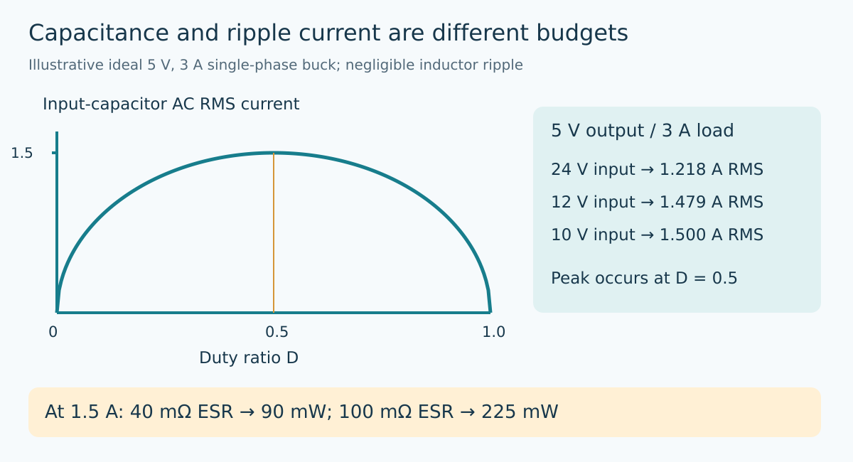
Input-capacitor RMS current = I × √[D × (1 − D)].
This is the alternating current in the ideal local input bank. It is not the converter’s average input current, and it is not the RMS value of the uncorrected rectangular switch current. Confusing those three quantities produces a plausible-looking but incorrect component budget.
Sweep the supported input range
Consider a hypothetical 5 V, 3 A gateway rail supplied from a variable low-voltage input. With D approximated by 5 V divided by input voltage, the predicted capacitor currents are:
- At 24 V input: D = 0.2083 and capacitor current is approximately 1.218 A RMS.
- At 12 V input: D = 0.4167 and capacitor current is approximately 1.479 A RMS.
- At 10 V input: D = 0.5 and capacitor current reaches 1.500 A RMS.
The worst point is not necessarily the highest input voltage. The function D × (1 − D) peaks at one-half. If the supported input range includes twice the output voltage, examine that point explicitly. If it does not, find the maximum within the actual operating interval rather than inventing an irrelevant test condition.
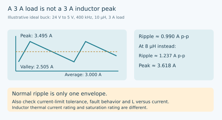
The simple waveform omits inductor ripple. For triangular peak-to-peak ripple ΔI in continuous conduction, the squared capacitor RMS current becomes I²D(1 − D) + DΔI²/12 under the same ideal-source assumptions. At D = 0.5 and ΔI = 0.9 A, the example rises from 1.500 A to approximately 1.511 A. This correction is modest here, but the assumptions should still be recorded.
Translate ripple into thermal stress
A first-order heating estimate is RMS current squared multiplied by equivalent series resistance. If the entire calculated 1.5 A passes through a hypothetical 40 mΩ ESR, dissipation is 90 mW. At 100 mΩ, it is 225 mW. These are electrical loss estimates, not temperature-rise predictions.
To turn them into a component decision, obtain the selected manufacturer’s ripple-current conditions, frequency corrections, temperature limits, and lifetime guidance. ESR varies with frequency and temperature, and a sealed enclosure changes heat removal. A rating printed at a different frequency or ambient condition cannot be transferred unchanged to the gateway.
Where harmonics matter, evaluate the relevant current spectrum and frequency-dependent impedance. One ESR value is a simplification. Likewise, a room-temperature case-temperature measurement alone does not establish the internal hot spot or lifetime at the product’s highest supported ambient.
Do not divide the current equally by capacitor count
A ceramic bank beside the switching loop and an electrolytic near the connector do not generally share alternating current in proportion to their capacitance labels. The sharing depends on impedance, mounting inductance, interconnect, and frequency. Two identical parts with asymmetric routing can also carry different currents.
TI’s application report emphasizes local ceramic decoupling and the effect of connection inductance. Treat that as a layout requirement, not permission to declare all ripple removed from the bulk capacitor. Build an impedance model or measure the branch currents with a method that does not substantially alter those branches.
For ceramics, use effective capacitance at operating bias and temperature. For bulk parts, separately check polarity, voltage margin, and the manufacturer’s permitted ripple. Adding capacitance can alter startup demand and input-network resonance; those are separate checks, not reasons to omit the RMS calculation.
Check voltage ripple with a different equation
The same simplified waveform gives a capacitive input-voltage ripple of approximately I × D × (1 − D) divided by switching frequency and capacitance. For 3 A, D = 0.5, 400 kHz, and 20 µF effective capacitance, that term is 93.75 mV peak to peak.
This excludes the ESR step and inductive spikes. It also does not predict upstream cable resonance. A capacitor bank might satisfy a voltage-ripple target but fail thermally, or pass its current rating while allowing excessive voltage excursion. Keep both acceptance limits visible rather than selecting whichever calculation produces the more comfortable result.
Validate the bank, not only the schematic value
Plan low-voltage bench checks at maximum load, relevant input voltages, and supported thermal conditions. Capture input voltage at the converter, distinguish switching ripple from probe-loop pickup, and document the measurement bandwidth. Record the actual capacitor part numbers and population, including substitutions.
Compare observed waveforms with the assumed conduction mode. Pulse skipping, discontinuous conduction, current limiting, and multiphase operation require their own waveform model. Do not stretch the continuous-conduction equation to cover every operating state.
The release decision should state effective capacitance, branch ripple-current allocation, component temperature evidence, and remaining uncertainty. The practical design rule is simple: bulk energy, voltage ripple, and RMS heating are three requirements. A single microfarad number answers only part of the problem.
Topic provenance
The preserved Google Trends RISING row “industrial iot solutions,+110%,” worldwide, all categories, web search, July 19–October 19, 2026 supports the parent integration topic only. It does not establish search growth for this electrical mechanism or article title.