THVD2450 Gateway Ports: Budget the Time Before Fail-Safe Goes High
A gateway receiver described as fail-safe does not necessarily report an idle bus immediately. Some devices qualify a near-zero differential input for a defined interval before forcing their receiver output high. That interval can be much longer than normal receiver propagation. If firmware interprets the output as an instantaneous cable-health indication, the hardware feature and the software assumption are solving different problems.
The concrete example is Texas Instruments’ THVD2450, a 50-Mbit/s RS-485 transceiver. This article uses its published timing and input-current contracts to design a review worksheet. It does not report a tested network, diagnose a specific installation, or replace the electrical requirements for a particular bus.
Separate two paths through the receiver
In the THVD24x0 datasheet, SLLSF20B, revised October 2021, section 8.3.5 on printed page 13 describes a timed fail-safe response for open, shorted, or idle inputs. A sufficiently small differential input must persist longer than the entry delay before the receiver produces the fail-safe high state.
The ordinary receive path is different. It follows positive and negative differential thresholds with hysteresis. The receiver function table on page 14 also identifies an indeterminate region between thresholds. Do not replace that table with the simplistic rule “all small signals are immediately high.” The timed fail-safe condition has its own amplitude and duration requirements.
This distinction explains why an output can remain dependent on its previous history briefly after an active driver releases the pair. It also explains why ordinary data propagation delay cannot serve as the maximum latency of every idle transition. Use the specification that describes the event actually being budgeted.
Convert the qualification interval into protocol scale
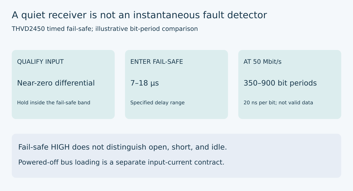
The THVD2450 switching table on page 7 specifies a fail-safe entry delay of 7 µs minimum, 10 µs typical, and 18 µs maximum with a 15 pF receiver-output load and the Figure 7-9 test arrangement. Its exit delay is separately listed as 25 ns minimum, 35 ns typical, and 50 ns maximum. These entries should not be merged into a symmetric generic “receiver delay.”
At 50 Mbit/s, one bit period is 1 / 50,000,000 seconds, or 20 ns. The 7–18 µs entry range corresponds to 350–900 such periods. At a hypothetical 115,200 bit/s, one period is approximately 8.681 µs, so the same entry range corresponds to roughly 0.806–2.074 periods.
The calculations do not predict an equivalent count of corrupt or missing bits. During a near-zero interval, there may be no valid transmitted data at all. Their purpose is to show that a component feature described in microseconds occupies very different portions of different protocol timelines. A product’s actual framing, idle definition, and receive filtering determine the consequence.
Use guaranteed bounds, not the typical 10 µs value, when establishing a required maximum wait under covered conditions. Conversely, a minimum entry delay may matter when deciding whether a brief event should have produced a fail-safe response. A single observed response time cannot substitute for either bound.
Do not promote a logic state into a fault classifier
A high receiver output is compatible with a valid high input, a qualified open bus, a qualified shorted bus, or a qualified idle bus. The feature deliberately makes several electrical situations produce the same logic result. It therefore cannot identify which one occurred by itself.
For a gateway health monitor, distinguish “no valid response arrived” from “the cable is open.” Combine protocol evidence with whatever independently justified diagnostics the actual product provides. A communication timeout may trigger a bounded retry or a maintenance alert, but it does not prove a particular physical fault.
Likewise, a stable high output after disconnecting a development cable is useful confirmation of one exercised branch, not proof that every short, supply state, or common-mode condition is covered. Keep the acceptance statement as narrow as the stimulus and source specification permit.
Powered-off loading is a separate worksheet
The electrical table on printed page 6 gives bus input-current limits with DE low and VCC either zero or 5.5 V. At a listed 12 V bus-input test point, the maximum is 125 µA. For 32 identical inputs at that same test condition, the arithmetic sum is 32 × 125 µA = 4 mA.
That is a single-line loading illustration at a specified voltage, not a differential termination calculation or a complete network node-count proof. It does not describe arbitrary fault voltage, unequal input voltages, added protection devices, or unspecified partially powered states. It does demonstrate that an unpowered device need not be an electrically absent device.
Do not confuse that bus current with receiver-output leakage or supply current in shutdown. They refer to different pins and states. Nor does fail-safe high mean that a powered-off receiver output is available to the host. The logic behavior and the load imposed on the cable need separate evidence.
Plan captures around the qualifying event
Use a controlled, current-limited low-voltage fixture and permitted input conditions. Observe the differential input and receiver output together, along with supply and enable states. Define the amplitude window and the interval’s start from the selected datasheet test circuit, not from a software message saying that transmission ended.
A useful plan compares an input that enters and remains in the qualifying window with one that returns to valid data before qualification completes. Also examine entry from both prior logic states. Preserve the differential waveform because a decoder alone cannot show whether the electrical dwell condition was satisfied.
Test shutdown and receiver disable as separate states, rather than interpreting a high-impedance output pulled high by the host as a fail-safe result. Use the actual input load and receiver-output capacitance when comparing with switching-table conditions. Avoid claiming a measured timing guarantee from an unreviewed fixture.
The deliverable is a two-path timing diagram, a state-specific loading calculation, and an explicit mapping from observations to permitted conclusions. Fail-safe logic can simplify a gateway interface, but only after its amplitude, dwell time, supply, and enable preconditions are carried into the system contract.
Source and demand context
Primary source: TI THVD24x0 datasheet, SLLSF20B, October 2021, electrical characteristics page 6, THVD2450 timing page 7, and functional descriptions pages 13–14. PDF and relevant page snapshots are preserved locally. All arithmetic examples and proposed checks are original, not measured results.
The preserved Google Trends export records “industrial iot solutions” rising 110% under “industrial iot,” Worldwide web search, all categories, July 19–October 19, 2026. This is parent-topic evidence only, not title-specific or THVD2450 demand evidence.