STM32F401CCU6 Temperature and VBAT Readings: Resolve the Shared ADC18 Path Before Building a Scan
Two scan ranks labeled “temperature” and “battery” do not create two internal analog inputs on the STM32F401CCU6. Both measurements use ADC1_IN18. If both source enables are set, the reference manual says the ADC converts the battery path. A temperature formula can then produce a plausible-looking number from the wrong physical signal.
The scope here is F401xB/xC, specifically F401CCU6, using RM0368 Rev 6, January 2025, DS9716 Rev 11, April 2019 and ES0222 Rev 9, February 2025. This is source analysis and an acquisition-plan review. No ADC firmware, sensor switching, calibration or electrical measurement was executed.
Establish the signal before interpreting the count
The datasheet explicitly connects this device’s temperature sensor to channel 18. That part-specific statement resolves the reference manual’s generic temperature-channel wording, which mentions channel 16 or 18; its Figure 38 footnote identifies channel 18 here.
The battery path reaches the same input through a divider. Setting VBATE in ADC_CCR connects VBAT/4 to ADC1_IN18. The ADC therefore measures the divided voltage, not the undivided battery voltage.
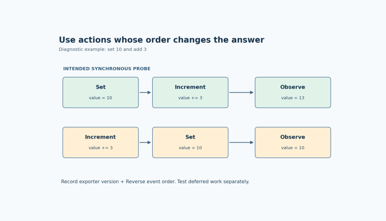
TSVREFE enables the temperature sensor and VREFINT. The register note requires VBATE to be disabled when TSVREFE is set and states that simultaneous enables select only the battery conversion. Treat that outcome as a documented conflict, not a useful combined operating mode.
For diagnosis, distinguish three labels: the application’s requested quantity, the configured channel number and the physical source presently connected to that channel. Only the third tells you what the acquired count represents. Averaging more samples cannot repair a mismatch between those labels.
Understand why another scan rank does not help
A rank specifies where a channel appears in a conversion sequence. It does not, by itself, execute a source-enable change between conversions. Two ranks selecting channel 18 therefore revisit the selected source; they do not alternate between the sensor and battery merely because software gives their destinations different names.
The same issue survives separation into two tasks or driver wrappers. Those abstractions still configure the shared hardware. A task-local structure is not an independent copy of ADC_CCR, and a lock covering only result-buffer access leaves source selection uncoordinated.
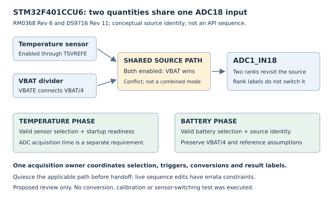
Use one acquisition owner to define complete, mutually exclusive measurement phases. Its responsibility includes source selection, trigger admission, conversion state, timing and result identity. This is an application design requirement inferred from the documented shared path, not a claim that a particular HAL sequence has been verified.
Make the handoff an explicit acquisition boundary
A proposed temperature phase admits results only after the valid sensor selection and required readiness conditions are established. A battery phase similarly owns its source configuration and labels its results as the divided battery path. Any reference measurement must occupy a separately valid configuration and timing window; do not assume VREFINT remains available with the battery selection.
Before changing the source or sequence, finish or quiesce the applicable conversion and trigger path according to the selected implementation. A queued hardware trigger, an in-flight conversion and a completed DMA buffer are different states. Define how the owner handles each rather than treating a register write as an atomic transaction boundary.
ES0222 section 2.4.1 adds a concrete constraint: modifying sequence registers during a software-triggered conversion resets that conversion without automatically starting the replacement sequence. The documented hardware-trigger behavior differs. The limitation applies across the listed silicon revisions A, 1 and Z. It is another reason to review the complete handoff instead of rewriting a live sequence and assuming continuity.
No exact stop, reconfigure and restart API recipe is prescribed here. That requires the actual trigger mode, DMA policy, driver revision and applicable errata handling.
Budget startup and sampling separately
DS9716 Table 72 gives a temperature-sensor startup time of 6 microseconds typical and 10 microseconds maximum. It separately specifies a minimum ADC sampling time of 10 microseconds for its stated temperature-sampling accuracy condition. Both timing entries are guaranteed by design.
Waiting for sensor startup does not lengthen the ADC acquisition interval. Translate the selected sample-cycle setting using the actual ADC clock, then check that interval against the documented requirement. Revisit the calculation when clock or prescaler settings change.
That sampling condition is not a guarantee of complete absolute temperature accuracy. Device variation, reference conditions and other error sources still matter; ES0222 also identifies internal noise affecting ADC accuracy. Selecting the correct source solves an identity problem, not the entire measurement error budget.
Keep evidence attached to each phase
A proposed read-only configuration trace should record source-enable state, selected rank, trigger and conversion state, actual ADC clock and the result’s phase label. Preserve the reference assumptions used for later scaling, including the battery divider.
A subsequent safe fixture could compare phase results with independently known battery and temperature behavior. Until such work is performed, describe it as planned validation. The immediate review succeeds when every result can be traced to one valid source configuration, rather than merely to a variable named after the intended measurement.