STM32H563 HSLV GPIO Mode: Qualify the I/O Supply Before Enabling the Speed Boost
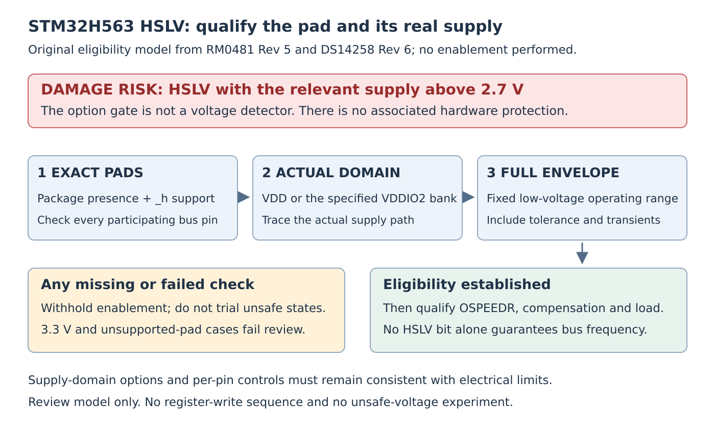
Enabling HSLV while the relevant I/O supply is above 2.7 V can damage the STM32H563. It is not a generic “fast GPIO” setting to add to a 3.3 V board. Eligibility depends on the selected pad, its actual supply domain and the supply’s complete operating envelope.
This review uses RM0481 Rev 5, July 2026 and DS14258 Rev 6, May 2025, scoped to STM32H563. No GPIO write, option-byte operation, supply change, electrical measurement or speed test was performed. The outcome is an eligibility worksheet, not an executable register recipe.
Identify the rail behind each pad
Begin with the selected package and the complete signal group. For every pin, record its package presence, I/O structure, alternate function and physical supply connection. A processor core-voltage setting cannot establish the voltage powering an output pad.
The datasheet identifies VDDIO2 for PB8, PB9, PD6, PD7 and PG9 through PG14; availability still depends on the package. Do not extrapolate that independent bank to every GPIO. Follow the exact package’s supply arrangement, including whether a dedicated supply pin is exposed or the domain is tied elsewhere.
For a proposed bus, the relevant question is not whether the board has a “1.8 V” rail. It is whether each participating pad is actually supplied from the qualified rail. A schematic net label, firmware voltage variable and measured pad-domain supply are different evidence. Keep their association explicit.
Check pad capability before speed settings
The I/O structure suffix _h identifies HSLV capability. RM0481 requires unsupported pins’ HSLV configuration to remain at reset, and likewise treats unavailable package pins as reserved. A uniform register mask across an entire port is therefore not an acceptable capability check.
ST’s STM32H5 GPIO training, read on October 19, 2026, also cautions against enabling the mode for a communication peripheral unless all its participating I/Os support it, because mixed capability can introduce timing side effects. The training has no identified printed revision; the reference manual and datasheet remain the version authorities.
Apply this check to the chosen routing, not merely the peripheral’s name. Moving one bus signal to a different alternate-function pin can change the eligibility result without changing the peripheral instance or intended clock rate.
Treat the option bit as a configuration gate
GPIOx_HSLVR provides per-pin control, gated by the corresponding IO_VDD_HSLV or IO_VDDIO2_HSLV option. The option definitions themselves require the respective supply to remain below 2.7 V when enabled. This is not a voltage sensor that decides whether a requested setting is safe.
The manual explicitly states that the feature has no associated hardware protection and recommends static configuration with a fixed I/O supply. A boot-time low-voltage reading does not establish safety after a regulator setting, power-source change or fault raises that rail.
Datasheet Table 20 lists 2.7 V as the HSLV-enabled operating maximum, while the register description says to use the mode below 2.7 V. Do not resolve that wording by designing a nominal rail exactly at the rounded boundary. Account for tolerance, ripple and transients, and retain margin within the applicable operating conditions. Absolute-maximum ratings are not a substitute.
Reject unsafe cases on paper
Consider four hypothetical review outcomes. A supported, fixed low-voltage pad group can proceed to detailed qualification once its full rail envelope is established. A group supplied at 3.3 V must reject HSLV enablement. A variable rail that can rise above the permitted range fails the static eligibility assumption. A low-voltage group containing unsupported participating pads fails the capability check.
These are configuration-review cases, not instructions to exercise the rejected combinations. In particular, do not enable HSLV on a 3.3 V fixture to see whether it survives. A device that appears functional after an invalid setting does not establish absence of damage or a supported operating condition.
If the intended routing fails, review the pin assignment or interface design within the product’s normal engineering process. Do not bypass the option gate or change supply architecture simply to clear a firmware configuration obstacle.
Qualify timing only after eligibility
HSLV, OSPEEDR selection and I/O compensation are different controls. The datasheet’s output-timing tables distinguish HSLV state and include supply range, speed selection and capacitive load; their notes and compensation conditions matter. No standalone HSLV setting guarantees a particular bus frequency.
After the electrical and capability checks pass, evaluate the complete peripheral timing budget: transmitted edges, receiving-device requirements, routing and actual loading. Preserve the exact table row and conditions behind each timing claim. Later measurements should use only approved, documented operating conditions.
The review record should name the device/package, every participating pad, its supply source and worst-case envelope, HSLV support, applicable option domain and timing assumptions. An unresolved supply or capability entry is a reason to withhold enablement, even when the register interface appears straightforward.