STM32WB Flash Writes During Radio Activity: Review PESD and the Semaphore Protocol Together
A local critical section does not give an STM32WB55 application exclusive control of flash timing. CPU2 can be serving the radio while CPU1 prepares a write, and both processors depend on the same flash bank. The flash driver must participate in the documented inter-core protocol.
AN5289 Rev 18 describes that protocol, including a detail often lost in abbreviated examples: CPU2 normally protects BLE timing through PESD, rather than semaphore 7 alone. This article reviews the admission and completion boundaries. It provides no erase command and reports no hardware timing test.
Begin with the resource that both cores need
AN5289 section 4.7 explains that the processors share a single flash bank. Programming or erasure prevents instruction fetch from that bank. Code executing from SRAM can avoid that particular fetch dependency only while it also avoids flash data accesses.
The note additionally states that CPU2 cannot execute code from SRAM in this architecture. Moving CPU1's programming routine into SRAM therefore does not solve CPU2's radio-timing problem. Nor does masking CPU1 interrupts stop CPU2 from needing the flash interface.
The RM0434 Rev 16 reference manual provides the flash and hardware-semaphore register contracts. Use those alongside the application-note sequence, rather than treating an isolated semaphore acquisition as the entire protocol.
Keep ownership and timing permission separate
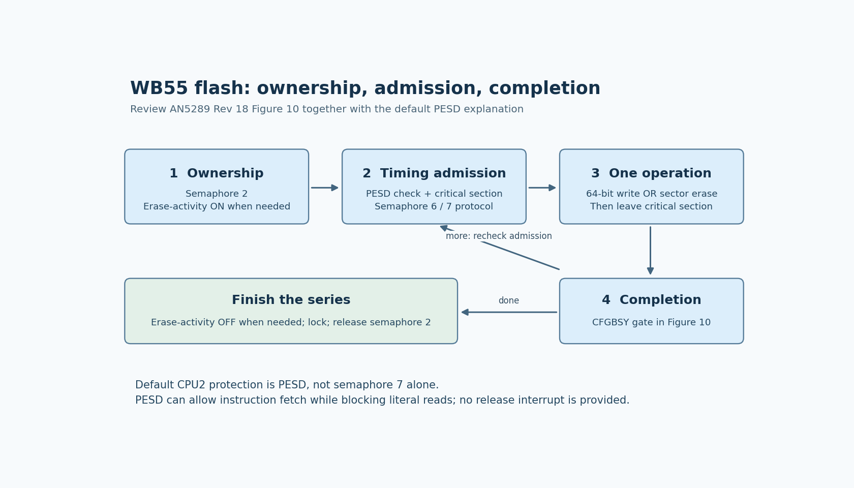
AN5289 Figure 10 starts with semaphore 2, which grants flash-operation ownership across the processors. That ownership spans the driver's work and is released when access is no longer needed. It answers who is using the flash programming interface, not whether the next operation is compatible with radio timing.
Semaphore 6 represents CPU1 timing protection against flash activity. Semaphore 7 supports CPU2 timing protection in the corresponding operating mode. The figure checks semaphore 6 and attempts semaphore 7 within the protected admission section, allowing only one 64-bit write or one sector erase before releasing and leaving that section.
A driver that acquires ownership once and then erases many sectors inside a long local critical section changes this contract. The documented loop revisits admission for each operation. Its structure gives timing protection a chance to affect subsequent work.
Read the PESD default before interpreting semaphore 7
The text following Figure 10 says CPU2 uses PESD by default to protect BLE timing. In that configuration, semaphore 7 checking does not provide the relevant protection by itself. CPU1 can select the mechanism through the documented SHCI_C2_SetFlashActivityControl command, which ST recommends configuring during initialization.
PESD also has a subtle CPU1 consequence. If it becomes set as CPU1 starts an operation, code fetching can continue while flash literal reads remain blocked. A short instruction trace that appears to run is therefore not proof that the application's complete path remains unstalled. Constants and compiler-generated literal accesses matter.
The note says there is no interrupt on CPU2's release of PESD. Do not design a nonblocking driver around an assumed PESD-release interrupt. Use the supported mechanism for the selected configuration and account for its actual progress requirements.
This is why a trace should record the configured protection mode. A semaphore-7 observation interpreted without that mode can lead to the wrong explanation for a delay or for apparent permission to program.
Announce erase activity and wait for actual completion
Before a series of sector erases, the driver must send the documented erase-activity-on command. After the relevant erases, it sends erase-activity-off. AN5289 recommends bracketing the series rather than sending the pair for every individual erase.
These system commands are outside the local critical section shown in the figure. Their role must remain separate from acquiring flash ownership and from executing an individual hardware operation. A wrapper that sends a system command while holding an unrelated long critical section needs its own communication-context review.
With the default PESD mechanism, AN5289 requires the flash driver to poll CFGBSY or read back until the programmed value is present. Figure 10 uses the CFGBSY completion gate before the next operation. A CPU-side function returning from an admission sequence is not sufficient evidence that the operation has crossed that hardware boundary.
Review the driver by transitions, not by API names
For each write or erase path, locate the ownership acquisition, configured timing mechanism, single-operation critical section, completion check and ownership release. For erase paths, also locate both activity notifications and their error handling. Include early exits: a rejected admission must not fall through into an unprotected operation.
Then propose a qualification run on a sacrificial region of a recoverable board, with radio activity and independent timing observation. Exercise delayed admission and errors separately from ordinary completion. Do not infer transaction durability from this protocol; power-loss recovery and persistent-record format remain separate storage properties.
The desired result is an explanation of why each individual flash operation was permitted and when it completed. A critical-section macro or a successful low-load demo cannot supply that evidence on its own.