SPI Full-Duplex Reads: Account for Dummy Bytes and Receive Data During Commands
Map transmitted and received bits on the same clock timeline. SPI clocks both directions, but the peripheral protocol decides which received bits have meaning. Discarding “all command bytes” can lose valid response bits when command and response fields share a host byte.
Applicability: the concrete example is Microchip MCP3008 using the three eight-bit-segment framing in datasheet DS20001295E, section 6.1. Linux v6.12 SPI transfer semantics provide the host model. This article concerns receive alignment and simultaneous TX/RX, not chip-select continuity or general ADC accuracy.
1. Separate bus clocks from meaningful receive data
A host can transmit a useful command while the receive pin is high impedance, send ignored fill bits while receiving a result, or exchange meaningful information in both directions within the same byte. “Dummy byte” must identify which direction and which phase it describes. It is not permission to discard the corresponding receive storage automatically.
The Linux v6.12 SPI interface describes transfers as simultaneous read/write segments. A receive buffer collects clocked input; omitting it discards that input. The library does not know which bits the peripheral labels command, null, padding, or payload. That interpretation belongs in the protocol driver.
Create a two-lane worksheet with one column for each host byte and, where needed, its individual bits. Label MOSI fields and MISO fields independently. Include high-impedance or unspecified intervals without assigning them invented values. A logic analyzer may show zeros during such an interval because of the board’s bias, not because the protocol promises zeros.
2. Use a target where command and result share a byte
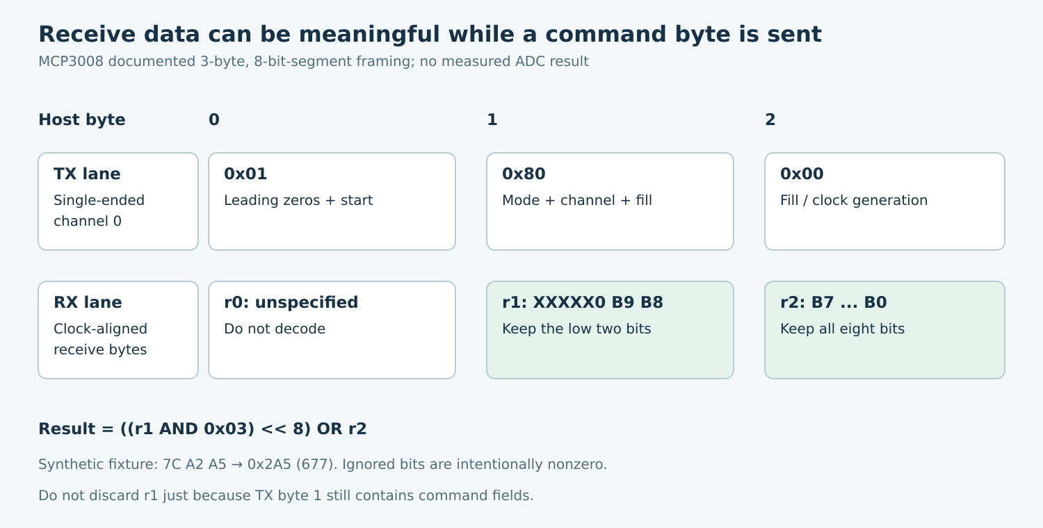
The MCP3008 datasheet shows a three-byte exchange with leading zeros before the start bit. In that arrangement, the second received byte contains five unspecified bits, a null bit, and the two most significant conversion bits. The third received byte contains the remaining eight result bits.
Meanwhile, the second transmitted byte carries the single-ended/differential selection and channel address before its unused positions. Therefore this byte cannot be treated as purely transmit-only. Discarding receive data until the third host byte throws away the upper two result bits.
For a hypothetical single-ended channel-zero request using the documented arrangement, the transmit bytes are 0x01, 0x80, and 0x00. The last byte supplies clocks rather than a second command. This is a framing example only; a real conversion also requires the specified supply, reference, input, acquisition, and serial timing conditions.
3. Define the decoder independently from the transfer API
Name the received bytes r0, r1, and r2 in clock order. For this exact arrangement, the ten-bit result is ((r1 AND 0x03) shifted left by 8) OR r2. Ignore the unspecified leading positions; do not copy the complete second byte into a larger integer and hope upper bits happen to be zero.
A synthetic receive fixture of 0x7C, 0xA2, 0xA5 should decode to 0x2A5, or decimal 677. The high bits of the first two bytes are deliberately nonzero so the fixture exposes an incorrect mask. These bytes are constructed software test data, not a captured ADC response or a claimed physical input voltage.
Keep extraction separate from scaling. First establish the raw ten-bit value and its range. Then apply the application’s documented reference and transfer function, with its error budget. A plausible voltage obtained after an incorrect shift is not evidence that the SPI framing was right.
4. Preserve receive storage during command transmission
The simplest host representation for this example is one three-byte full-duplex transfer with both transmit and receive buffers. Capture all three received bytes and decode afterward. This makes the lane map visible and avoids hiding meaningful bits behind a transmit-only helper.
If the implementation uses several segments, retain receive data from every segment containing meaningful response bits. Account for where each segment’s data lands in host memory. A second buffer beginning at offset zero is not automatically the same as the second byte of the overall exchange.
Check wrapper behavior carefully. Some APIs return only bytes from a later “read phase,” while others return the receive stream for the whole exchange. Document that contract at the driver boundary. Do not repair a wrapper mismatch by scattering unexplained plus-one and minus-one offsets through application code.
5. Test masks, offsets, and word boundaries
- Range endpoints: construct frames representing zero and the maximum ten-bit value. Verify exact extraction without sign extension.
- Upper-bit boundaries: test values around 0x0FF/0x100 and 0x1FF/0x200. These expose loss of the bits received during the second transmitted byte.
- Unspecified positions: vary the ignored bits while keeping payload bits fixed. The decoded value must remain unchanged.
- Offset faults: prepend or omit a synthetic byte and require the framing layer to reject the wrong length rather than decoding a plausible number.
- Channel selection: check each intended channel command against the datasheet and verify that channel identity travels with the decoded result.
A decoder unit test cannot prove that hardware generated the correct clocks. On the target, capture CS, SCK, MOSI, and MISO, then annotate the same byte and bit positions used by the fixture. Compare the raw received buffer with the capture before examining scaled application values.
6. Keep timing changes from becoming alignment workarounds
The MCP3008 is an ADC whose conversion progresses through the serial exchange. Its datasheet includes constraints beyond a maximum SPI rate, including limits associated with conversion duration. Do not insert arbitrary long delays to make a receive buffer look aligned. Clock grouping and timing must both remain within the target contract.
If the raw bytes differ from the sampled waveform, inspect host word width, phase, bit order, and buffer handling. If the bytes match but the extracted value is wrong, inspect the lane map and mask. If the raw result is correct but the voltage is wrong, investigate reference, analog input, and scaling separately.
The release artifact is a per-bit TX/RX map, a documented buffer-return convention, synthetic decoder fixtures, and target captures for representative channels and values. No MCP3008 conversion or Linux SPI operation was executed for this article. The constructed fixture specifies expected decoder behavior; it does not claim a tested driver or measured converter performance.