SPI Mode Mismatches: Diagnose Edge Selection Before Lowering the Clock
Translate the peripheral timing diagram into idle level, launch edge, and sample edge before changing SPI frequency. A clock rate reduction cannot make an incorrect edge contract correct. It may only make an accidental timing margin look reliable enough to hide the defect.
Applicability: the concrete device is Analog Devices ADXL345 in four-wire SPI, datasheet revision G. Linux SPI terminology supplies the host-mode mapping. The method applies to other devices only after their own timing diagrams are checked; do not transfer the ADXL345’s mode or electrical limits to another part.
1. Name physical edges before naming a mode
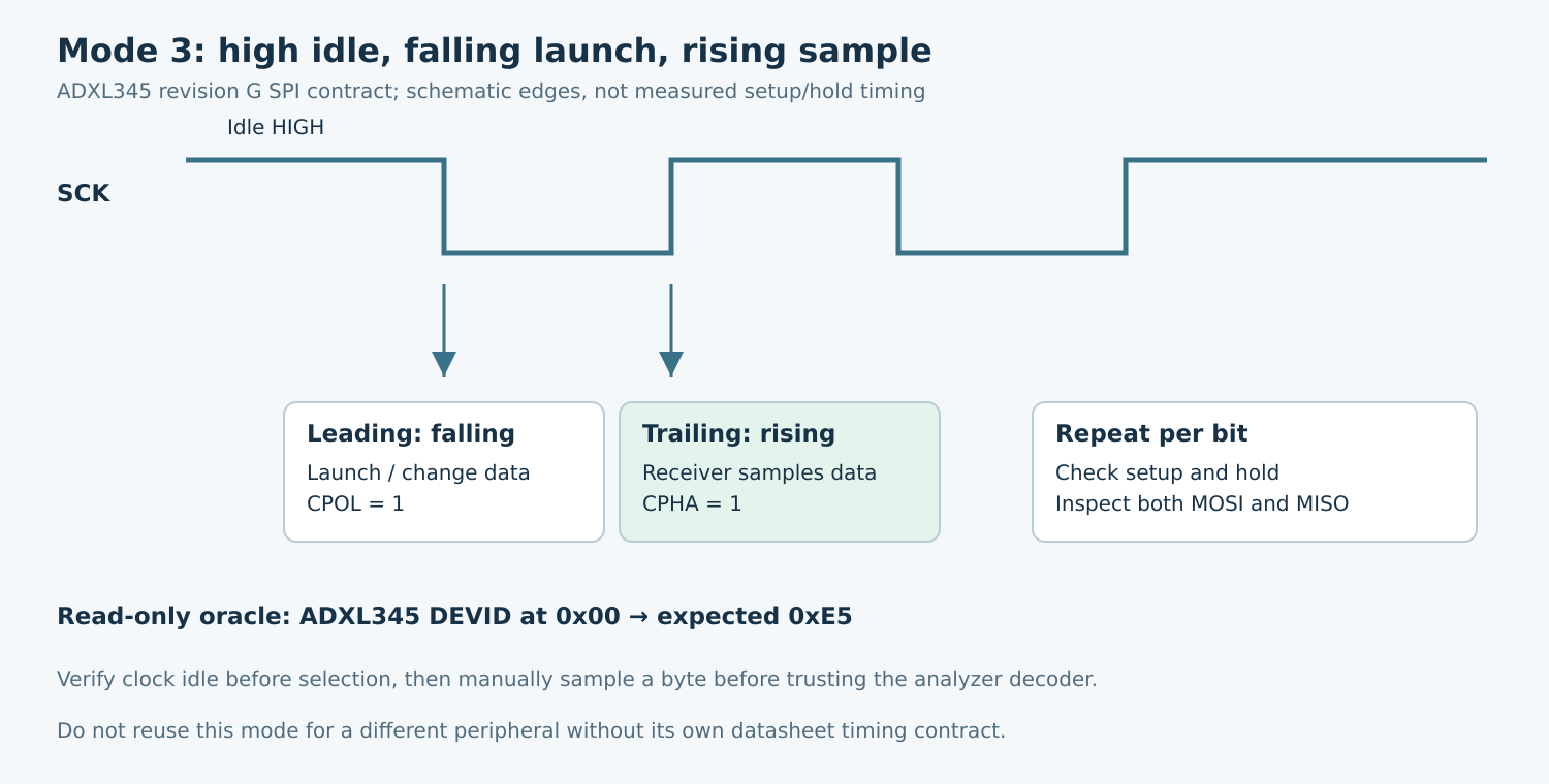
The Linux SPI overview defines CPOL as clock idle polarity and CPHA as whether sampling occurs on the leading or trailing edge. “Leading” means the first edge away from idle, so it can be rising or falling. A statement such as “sample on the second edge” is incomplete without the idle level.
The ADXL345 revision G datasheet specifies CPOL = 1 and CPHA = 1 for SPI. In the conventional mode numbering this is mode 3: clock idle high, first edge falling, sampling on the trailing rising edge. Record those physical facts beside the software constant.
Create a worksheet with separate MOSI and MISO rows. For each, identify the transmitting side, when data becomes valid, the receiver’s sampling edge, required setup and hold, and any first-bit exception. Add chip-select setup/hold and permitted clock frequency under the actual supply and loading conditions.
2. Check idle behavior at selection
Capture SCK before CS becomes active, not only the middle of a byte. An idle level that is corrected after selection can introduce an unintended first edge. Confirm that the controller applies the target’s configuration before selecting it, including when the previous transfer on a shared bus used another mode.
Check startup and resume separately. A bootloader, reset GPIO state, or power-management transition may leave the bus in a different condition from steady-state transfers. A read that succeeds only after another transaction has “warmed up” the bus deserves investigation of initial clock and chip-select behavior.
Do not infer the physical level solely from a configuration register or API readback. Those are useful records of intent. The target-side capture establishes what the selected device actually saw, including any inversion or delay through board components.
3. Use a deterministic register before live data
The ADXL345’s read-only DEVID register at address 0x00 contains 0xE5. It provides a useful initial response pattern with both ones and zeros. Use the documented read command for the selected interface and capture the command plus response. This verifies communication framing; it does not validate acceleration measurement accuracy.
A hypothetical test fixture can repeatedly read this identity while saving the raw received bytes and the mode configuration. Then add a documented stable register or a safely controlled test pattern where the product permits it. Avoid calibrations, resets, or writes to unrelated configuration merely to obtain an easy-looking pattern.
All-zero and all-one responses are weak timing tests. They may result from a floating line or fail to expose a bit shift. Choose patterns with transitions near the beginning and end of a word when a controlled write/read fixture is available. Keep the expected bit sequence separate from its displayed hexadecimal representation.
4. Decode one byte manually from the capture
- Identify the actual idle SCK level while CS is inactive.
- Mark the first clock edge after CS assertion and label it leading.
- Mark the selected sample edges using the target contract.
- Read the line value at each sample edge in the required bit order.
- Compare the resulting bits with the expected command or response byte.
- Measure data stability around the sample edges using the datasheet’s applicable limits.
Configure the analyzer decoder only after this exercise. Otherwise a decoder set to the same wrong assumption as the host can produce persuasive but misleading text. Preserve raw edges, especially around the first bit, the command/response transition, and the final bit before CS release.
Inspect MOSI and MISO independently. A correct command decode does not prove that the host samples the peripheral’s output correctly. Different output delays, routing, and level-shifter directions can leave one direction with margin and the other without it.
5. Distinguish mode, bit order, and electrical margin
A repeatable bit-position shift is a clue to framing or edge selection, but not proof. Reversed bit order, an extra clock, or a wrongly counted command byte can produce similar values. Compare the full bit sequence and field boundaries before diagnosing from one hexadecimal error.
If data changes near the host’s sample edge, compare the configured phase with the target’s launch edge. If the phase is correct but setup time shrinks as frequency rises, investigate propagation delay and electrical loading. If the clock rings across a threshold more than once, digital mode changes alone are not an adequate repair.
Lowering frequency is a useful controlled experiment after the mode is established. Record the prediction: more time between launch and sample should improve an actual timing-margin problem. If only the first bit remains wrong at every rate, inspect selection and first-edge handling before concluding that the device is too slow.
6. Test configuration transitions, not just one steady stream
On a safe development setup, repeat the documented identity read after cold start, host-controller reset, suspend/resume, and traffic to another SPI target using a different mode. Check that per-device configuration is restored before every selection. These transitions can expose bugs that a continuous same-device loop misses.
Use deliberately incorrect modes only as controlled negative tests with read-only operations and a known recovery path. Do not assume an invalid command is harmless on every peripheral. The acceptance criterion for the negative test is detection of a contract violation, not one mandatory error value.
For the final candidate configuration, retain the selected mode and word settings, target datasheet revision, waveform annotations, operating conditions, and test-case results. Require the first and last bits to satisfy the timing worksheet, not merely an expected byte returned on one attempt.
No ADXL345 transaction or timing measurement was performed for this article. The figure is a conceptual mode-3 edge map. The next step is to compare that contract with the actual board capture and qualify setup/hold margin under the product’s supported conditions.