STM32F401CCU6 Core Supply: Use the Single-VCAP Regulator Circuit for Its Package
A schematic copied from a larger STM32F401 package can contain the right family name and still implement the wrong core-supply circuit. For the STM32F401CCU6, identify the single exposed regulator-stabilization connection before choosing capacitors or investigating firmware startup.
This review uses DS9716 Rev 11, April 2019, specifically the regulator description, package pin table and power-supply diagram. The result is a package-specific net check. It does not establish a measured startup fault, capacitor qualification or board reliability.
Resolve the ordering code before copying the supply figure
The ordering information identifies U as UFQFPN. Combined with the selected pin-count code, STM32F401CCU6 uses UFQFPN48. In Table 8, its VCAP_1 connection is pin 22. Section 3.15.1 limits VCAP_2 availability to LQFP100 and UFBGA100.
The generic supply figure contains connections for multiple packages. It therefore cannot be copied literally as the footprint’s pin inventory. Start with the UFQFPN48 column and connect each actual supply pin to its documented role. An absent second VCAP connection does not mean the first connection is optional.
This distinction matters when a library symbol was originally built for a larger part. A hidden power pin, inherited net alias or unused-looking capacitor pad can conceal a topology error even when the bill of materials lists a familiar capacitance.
Trace two different capacitor networks
Figure 18 shows the external VDD network feeding the device and its internal voltage regulator. Separately, the regulator’s stabilization capacitor connects through VCAP to the ground return. These are different electrical nodes.
For the one-VCAP arrangement, Figure 18 specifies one 4.7-microfarad capacitor. Section 6.3.2 confirms that packages with one VCAP pin replace the two external capacitors with a single capacitor. Read those together rather than taking the two-pin value from Table 16 and applying it unchanged to the smaller package.
A separate 4.7-microfarad ceramic capacitor appears in the VDD decoupling network; the figure’s footnote connects that component to one VDD pin. Equal nominal values do not make the components interchangeable. A 4.7-microfarad capacitor installed only across VDD and VSS does not provide the required capacitor from VCAP_1 to VSS.
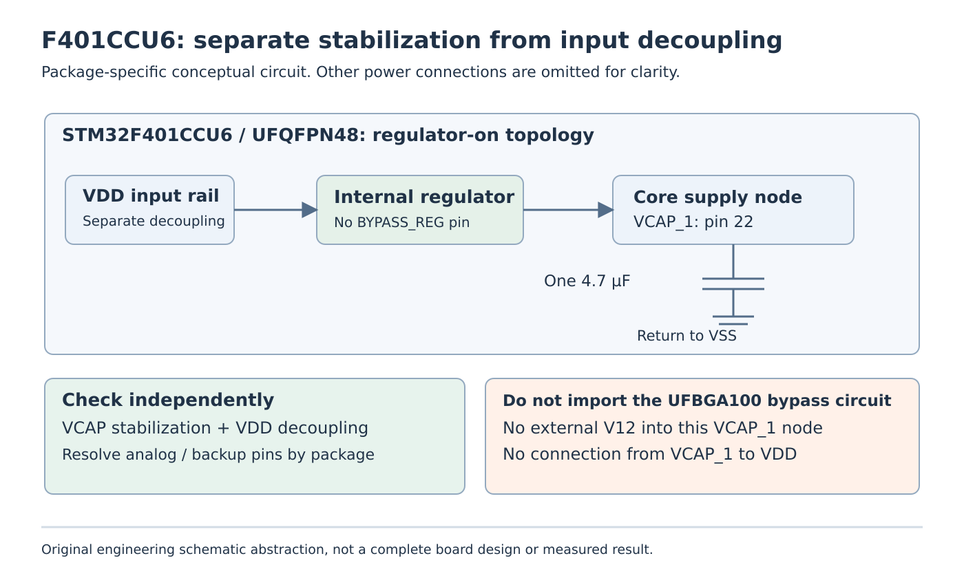
Follow both nets in the schematic and PCB. Confirm that the VCAP_1 capacitor actually returns to the intended ground connection and has not been joined to VDD by a reused label. Then inspect the separate decoupling at the real supply-pin pairs. The generic figure’s supply count is not permission to invent additional pins on UFQFPN48.
Table 16 explicitly describes its 2.2-microfarad and ESR entries for the arrangement with both VCAP_1 and VCAP_2 available. Do not cite that table as an independently stated single-capacitor qualification. Selecting the actual component and confirming its behavior under the board’s conditions remain engineering work beyond the nominal topology shown here.
Keep the rest of the supply circuit visible
A correct core capacitor does not complete the board’s supply review. Figure 18 also shows the analog supply and ground relationship, backup supply circuitry and the separate supply decoupling. Its note specifies VDDA = VDD and VSSA = VSS. Resolve reference and backup connections using the actual package rather than exposing every pin drawn in the family-level illustration.
The datasheet calls for ceramic filtering capacitors at each supply pair, placed as close as possible to the appropriate pins, including the permitted underside placement. Check those connections and physical returns together with the core capacitor. A schematic-only review cannot demonstrate that the layout meets the intended placement.
The useful artifact is a marked-up supply sheet: actual package pin, board net, capacitor connection and applicable datasheet figure or table. That sheet should distinguish input-supply decoupling from regulator-output stabilization without relying on component names such as “bulk” or “core.”
Reject the unsupported external-core-supply substitution
Section 3.15.2 makes regulator-off operation specific to UFBGA100, which exposes BYPASS_REG. That configuration supplies an external V12 through the two VCAP connections and changes the capacitor and supervision requirements. It is not another stuffing option for STM32F401CCU6.
For packages without BYPASS_REG, section 3.15.1 says the regulator is always enabled. The software-controlled main-regulator, low-power and Standby behaviors described under regulator-on operation do not create the missing external-supply bypass connection.
Consequently, do not adapt the UFBGA100 circuit by driving the CCU6 VCAP_1 node from an external core rail, tying it to VDD, or replacing its stabilization capacitor with the bypass circuit’s decoupler. A firmware setting cannot make that package support the documented regulator-off topology.
Finish with an unpowered connectivity review
Before energizing a revised board, compare the symbol, footprint, netlist and fitted components against this package-specific supply sheet. Flag a missing VCAP_1 capacitor, a shared VDD/VCAP_1 net, or an inherited bypass circuit as unresolved design discrepancies.
No board was powered or measured for this article. The immediate acceptance condition is narrower and useful: the chosen package implements its supported regulator circuit, with single-pin stabilization and input-supply decoupling independently accounted for. Electrical qualification follows that connectivity decision.