Gateway PCB Layer Changes: Follow the Return Current Through the Via Transition
A gateway PCB can satisfy a trace-width rule and still contain a poor high-frequency current path. When a signal changes layers, its nearby reference may change too. The signal via is easy to see in the layout; the route that lets return current move between reference planes is often less obvious. Reviewing only the copper carrying the named signal misses half of the transition.
Texas Instruments’ High-Speed Layout Guidelines for Signal Conditioners and USB Hubs, SLLA414A, revised January 2026, addresses return paths and reference discontinuities on pages 6–10. Its preferred arrangement keeps high-speed routing over solid ground reference, avoids splits, and uses nearby ground stitching when appropriate ground planes must be connected. The discussion here turns that principle into a board-review decision, not a universal via geometry or an EMC certification claim.
Read the stackup as part of the circuit
Start with the actual layer stackup rather than the colors in a routing screenshot. For each segment, identify the relevant adjacent reference conductors and their electrical nets. “Plane layer” is not enough: a ground region, a power island, and an isolated field-side reference are different electrical objects.
At high frequencies, return-current distribution is strongly influenced by the electromagnetic coupling between signal and reference. It should not be imagined as one thin wire taking an arbitrary shortest route, nor as DC current choosing only the lowest resistance. A continuous nearby reference gives the signal a predictable environment; a void forces a different field and current distribution.
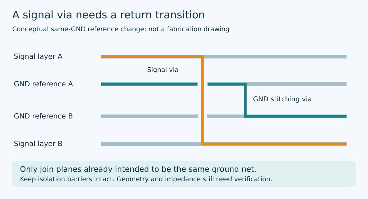
Create a short transition record for each critical net: starting signal layer, reference before the via, destination signal layer, reference after the via, and the intended connection between those references. This exposes an otherwise hidden question. A signal can move through a plated hole successfully while its return path must travel much farther to find a suitable connection.
Same ground net does not mean zero high-frequency distance
Suppose two separate ground planes are connected elsewhere on the board. They share a schematic net, but the path between them near a particular signal transition can still have significant inductive impedance. A nearby stitching via provides a local conductive transition between those same-net planes.
Placement matters because the goal is to avoid a large detour in the current loop. A stitching via at the opposite side of the enclosure is not electrically equivalent to one near the signal via just because both carry the label GND. Review the implementation in three dimensions, including antipads, plane clearances, and the actual layers that each via reaches.
For differential pairs, preserve a balanced environment around the two signal transitions. Symmetry does not mean that an ideal differential pair eliminates every reference-current concern. Real launches, skew, imbalance, and common-mode content still need a return path. Apply the interface and component vendor’s detailed constraints rather than inventing a generic number of ground vias for every pair.
Use an inductance example to understand the cost
The simple relationship V = L × di/dt illustrates why a small additional inductance can matter during a fast edge. Assume, purely for explanation, a current change of 20 mA in 1 ns. That is a rate of 20 million amperes per second.
A modeled 2 nH inductance produces 40 mV from that rate of change. A modeled 10 nH produces 200 mV. Those values do not assign an inductance to a particular via spacing or predict a receiver’s measured glitch. They show why a connection that looks adequate in a DC continuity test can have an important transient effect.
The calculation also separates edge speed from repetition rate. Sending the same fast edge less often does not automatically reduce the instantaneous di/dt of each transition. A low-frequency control signal can therefore deserve careful return-path treatment when driven by a fast output. Reducing traffic may change observed failures without repairing the underlying geometry.
Different reference nets require a different decision
Never insert a ground stitching via between two planes merely because both appear beneath signal routing. If one plane is a power rail, that connection would be a short. If the planes belong to opposite sides of an isolation barrier, it would defeat the isolation architecture. Net names, schematic intent, clearance requirements, and barrier boundaries must be checked before any copper change.
The TI guide discusses capacitive return paths where reference changes cannot be avoided. That is not permission to bridge an isolation barrier with an arbitrary capacitor. For ordinary nonisolated power-to-ground reference changes, the full decoupling and impedance arrangement needs analysis. For safety isolation, any allowed capacitance belongs to the approved insulation and leakage-current design, with suitable components and engineering review.
Prefer a routing or stackup arrangement that avoids the problematic reference change when practical. A local capacitor is not a universal eraser for a split plane: its mounting inductance, connection geometry, and frequency response remain part of the path. Do not choose a capacitance solely because its low-frequency reactance looks small.
Check the manufactured geometry, not just connectivity
Plane voids may come from connector fields, antipads, mounting clearances, or power partitioning rather than an obvious intentional split. Display the reference layer underneath the entire critical route, including the launch and receiver approach. A trace can be continuous while crossing a hole in the conductor that was supposed to reference it.
After layout changes, confirm that the fabrication output retains the intended plane connections and clearances. A stitching via with a thermal-relief or clearance arrangement different from the reviewed model can change the implementation. The conceptual illustration deliberately omits detailed antipads and dimensions; it is not a manufacturing drawing.
Close the review with a transition map and an evidence plan appropriate to the interface. Simulation, impedance characterization, receiver-side waveform inspection, and emissions testing answer different questions. Use them where the product requires them, preserving stackup and build conditions. Passing a connectivity check proves the intended nets connect; it does not prove that fast return current has an acceptable route.
Primary reference and trend scope
Texas Instruments SLLA414A, January 2026 revision, return-path and reference-discontinuity guidance, pages 6–10. The inductance example is hypothetical arithmetic, not extracted PCB parasitics or measured performance.
The preserved Google Trends RISING row “industrial iot solutions,+110%,” worldwide, all categories, web search, July 19–October 19, 2026 supports the industrial-gateway parent topic only. No rise in demand for PCB stitching vias or this title is claimed.