LVGL 9 DMA Display Corruption: Flush Completion, Cache Coherency and Buffer Ownership
Classify the visible failure before changing cache settings
A display that works synchronously but fails with DMA has exposed a timing or memory assumption. Begin with a static border and a moving solid block. Damaged pixel values, a horizontal discontinuity during motion, and repeated old content suggest different investigations. Preserve a short video and the exact build, then note whether the failure follows DMA enablement, a memory-region change or cache enablement.
The LVGL API reference here is v9.3.0, with v8.3.11 as the migration baseline. This article describes a review and test method, not a validated driver for every MCU. Before testing, list the processor, display interface, DMA controller, source RAM region, cache policy and actual cache-line size. A DMA engine that cannot reach the chosen RAM cannot be repaired by adding a cache operation.
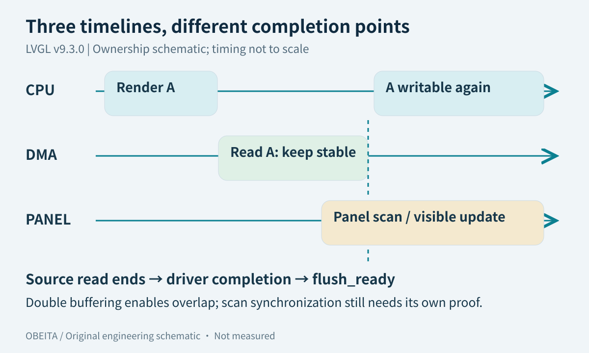
Draw rendering, transfer and scanout as separate timelines
Give each buffer an explicit owner. While LVGL produces pixels, the CPU may write it. After submission, the transport reads a fixed byte range, and that range must remain stable until the driver releases it. The panel may scan its internal memory later. A source buffer can therefore become reusable before all those pixels are visible on glass.
For an SPI panel with internal display RAM, track source consumption and bus transaction completion according to the peripheral driver. For a continuously scanned framebuffer, track which frame is being scanned and when a page-flip latch actually takes effect. Double buffering permits overlap only when these ownership transfers are correct. It does not automatically synchronize updates with the panel scan, and a tearing-effect signal has meaning only within the panel’s documented timing contract.
Prove the instant at which flush completion is reported
Instrument three events with a fixed-size trace buffer or GPIO: submission, the relevant hardware completion, and lv_display_flush_ready. Attach a monotonically increasing transfer identifier and source address. The identifier lets you detect a delayed interrupt belonging to an earlier transfer instead of accepting it as completion of the current one.
For the normal completion mode, report ready only when the driver is finished with the source. The v9.3.0 display header also defines a flush-wait callback; that is a separate integration choice, and its waiting contract must be reviewed instead of mixing completion designs. The outline below is pseudocode, not compiled interrupt code.
on_flush(display, area, pixels):
    require(state == IDLE)
    save_transfer_id_and_source_range()
    prepare_source_for_device_if_required()
    state = IN_FLIGHT
    submit_transfer_or_enter_fault_recovery()

on_matching_completion():
    require(source_is_no_longer_read_by_hardware())
    finish_required_bus_handshake()
    state = IDLE
    lv_display_flush_ready(display)

on_error_or_timeout():
    stop_and_quiesce_the_actual_hardware()
    reject_stale_completion_events()
    recover_or_keep_display_in_fault_state()
Every error path needs a deliberate decision about recovery. Merely timing out does not stop DMA. Do not return ownership while a controller may still read the old address, and do not call ready twice for one submission.
Review cache maintenance in the direction of data flow
When a CPU has produced pixels in a non-coherent, write-back cached region and DMA reads physical memory, dirty cache contents may need cleaning before the device starts. Invalidation has a different purpose and can discard CPU modifications if used incorrectly. An instruction-cache operation does not substitute for data-cache visibility.
Use the target vendor’s memory and DMA rules for the maintenance range, barriers and ordering. ST AN4839 is relevant to the STM32F7/H7 families it covers; it is not a universal recipe for every STM32, ESP32 or Linux system. On Linux, use the platform’s DMA mapping interfaces rather than importing bare-metal cache calls.
Allocate dedicated cache-line-aligned storage where required, including the end boundary. Expanding a range to full cache lines can touch unrelated data if buffers share a line. A working uncached-memory experiment can narrow the hypothesis, but it does not prove the final cached configuration safe or justify changing MPU attributes without reviewing all users.
Audit both buffer addresses and lifetimes
Check that A and B really refer to independent allocations, remain alive during asynchronous use and reside in DMA-accessible memory. A local stack array can look correct in a debugger while becoming invalid as soon as its function returns. Confirm alignment, capacity and actual linker placement in the release build, not only the debug build.
| Observed condition | Likely boundary to inspect | Decisive next observation |
|---|---|---|
| Corruption begins after early ready | Source ownership | Write begins before DMA source read ends |
| Only cached RAM fails | Visibility or shared cache lines | Compare dedicated aligned storage |
| Stable horizontal split during motion | Panel scan synchronization | Compare scan/TE timing with writes |
| Display stops after one update | Missing completion or error path | Submission has no matching release |
| Old transfer completion arrives late | Recovery bookkeeping | Transfer identifier mismatch |
For page flipping, retain the previously displayed framebuffer until hardware confirms that it no longer scans it. For SPI, preserve command/data and chip-select sequencing even if the DMA source itself is already consumed. Those are related but distinct lifetimes.
Find the smallest failing configuration
Keep one deterministic UI workload and change one variable at a time: blocking versus DMA, one versus two buffers, one approved memory policy versus another. Do not simultaneously change panel frequency, compiler optimization and allocation location. Record the exact number of transitions, corruption count, timeout count and test duration; “ran for a while” makes regression comparison unreliable.
Add controlled interrupt load on a recoverable development board and repeat transfers that cross row or cache-line boundaries. Avoid logging every pixel or printing from a critical ISR, since the diagnostic can create the timing problem it is meant to explain. Capture the same trace before and after a candidate fix. A higher apparent update rate obtained by announcing completion early is a correctness defect, not a performance improvement.
Deliver the ownership proof and its limits
A useful repair package contains the buffer map, ownership state diagram, completion-event definition, successful and failed transfer paths, and a trace showing that writes do not overlap outstanding source reads. State the tested board revision, RAM region, SDK and cache configuration. Mark untested reset, timeout and scanout paths explicitly.
If synchronous output is also wrong, return to the migration and pixel-format checks. Once correctness holds, carry rendering and transfer timestamps into display performance profiling. Keep a low-overhead diagnostic switch so a later field failure can be compared with the same event definitions.
For a display-driver diagnostic review, share sanitized flush and completion code, the RAM map, cache settings and a short trace. The review should end with a platform-specific ownership contract and a test plan; this article supplies no measured FPS gain or cross-chip guarantee.